
Homework Answers
Add Answer to:
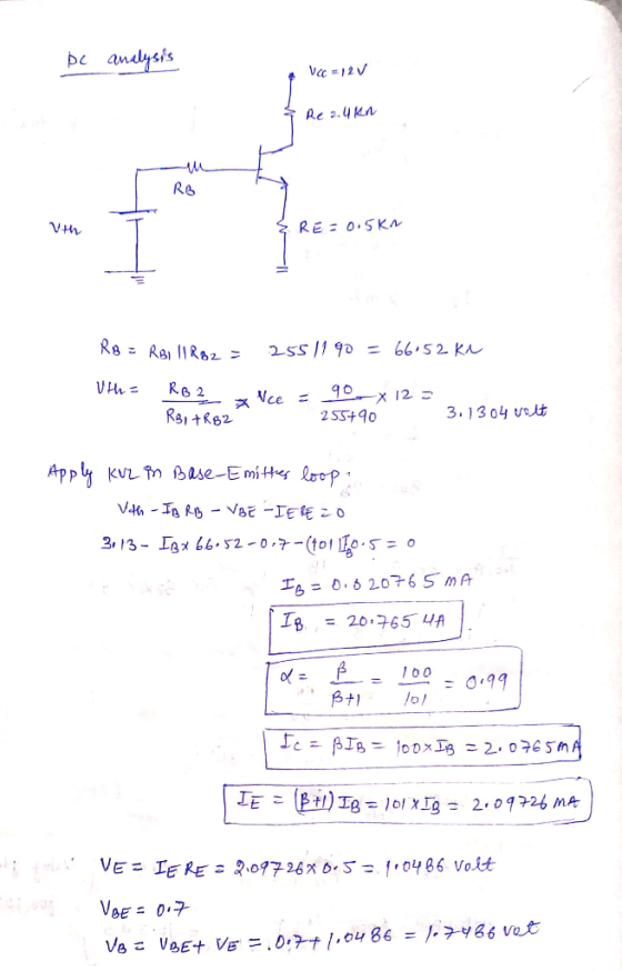
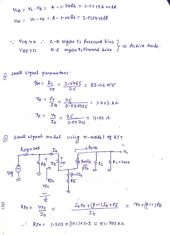
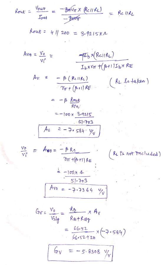
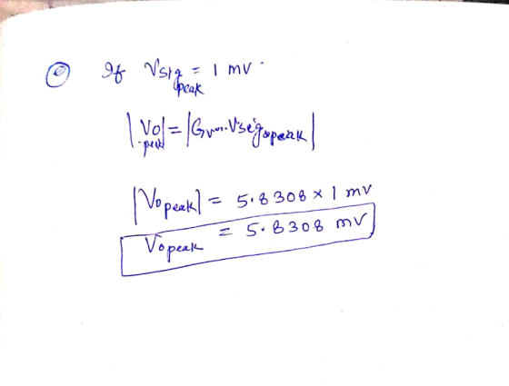
slove please Name/Date: 2. Given the npa BJT common emitnter amplifier circuit in Figure 2, assume e given below, and determine the following a) [DC Analysis] Find: α-- -h" V. Va and VCE Use ab...
Shown below is a single stage common emitter amplifier with a unipolar dc power supply using an 2...
 Shown below is a single stage common emitter amplifier with a unipolar dc power supply using an 2N3904 NPN BJT as the active device. It is specified that V+ 40 V, C1 C2CE 100uF, Ro-7.5 k2, REi-5.1kS2, and Ri - 36k52. Design the circuit so that the dc collector current is 2 mA and the magnitude of the small-signal midband voltage gain is 32.3. For the design calculations assume that the base-to- emitter dc voltage drop is 0.65 V, the...
FIND THE VALUES OF Rb1, Rb2, Re,Rc, rin , rout, overall gain and open circuit gain First, design a common emitter BJT a...
 FIND THE VALUES OF Rb1, Rb2, Re,Rc, rin , rout, overall gain and
open circuit gain
First, design a common emitter BJT amplifier Second, analyze the amplifier.( Avo, Gv, Rin, Rout) Third, compare your calculation with Multisim. Report must include comparison between your calculation & simulation results overall voltage gain, open circuit voltage gain, input resistance, and output resistance. This design project is not group work, must be done individually. Type your report. Design a discrete common emitter BJT amplifier.(Determine...
FIND THE VALUES OF Rb1, Rb2, Re,Rc, rin , rout, overall gain and
open circuit gain
First, design a common emitter BJT amplifier Second, analyze the amplifier.( Avo, Gv, Rin, Rout) Third, compare your calculation with Multisim. Report must include comparison between your calculation & simulation results overall voltage gain, open circuit voltage gain, input resistance, and output resistance. This design project is not group work, must be done individually. Type your report. Design a discrete common emitter BJT amplifier.(Determine...
4. Consider the following Common Base BJT circuit given in the figure below: i. Use the...
 4. Consider the following Common Base BJT circuit given in the figure below: i. Use the data sheets of CA3046 BJT array and design a common collector circuit given in the following Figure 2 with the stated specifications in Table 2 Clearly show your design procedure. (Hint: show your calculation steps for both DC and AC small signall analysis) ii. Important Note : Ifyou remove RE you should also remove ClI, that is, connecting ac voltage source directly to emitter)...
Problem 2: BJT Small-Signal Voltage Amplifiers in the lectures, we covered in detail the analysis of an npn BJT amplifier that utilizes a single-supply DC biasing. In this problem, you will meet...
 Problem 2: BJT Small-Signal Voltage Amplifiers in the lectures, we covered in detail the analysis of an npn BJT amplifier that utilizes a single-supply DC biasing. In this problem, you will meet two additional amplifier architectures- one that is based on dual DC supplies combined with a DC current source, and the other that utilizes a pnp BJT with single-supply biasing. In both problems (below) you need to manually find the amplifier's Q-point (that is, the DC values of Ic...
Avec Úvo SRE L V II. (5pt) Consider the above-right common-collector or emitter-follower BJT amplifier circuit....
 Avec Úvo SRE L V II. (5pt) Consider the above-right common-collector or emitter-follower BJT amplifier circuit. Given: ß= 100, RE = 10 k1, Vcc = 20 V, RB = 5 k1, R1 = 10 kl, and Ry = 2 k1. (a) (1pt) Find the Q-point, i.e. Ibo, Ico, and VCEO; (b) (1pt) draw the small-signal equivalent circuit assuming that the capacitors (C, and Cy) are short circuits for the small signal; (c) (1pt) solve for the voltage gain, Av; (d)...
2. For the common-emitter amplifier. B= 50. Vcc=12 a) Draw small signal circuit b) Find vout/vin...
 2. For the common-emitter amplifier. B= 50. Vcc=12 a) Draw small signal circuit b) Find vout/vin Find Zin and Zou Vcc R1 27k R2 2.2k Zout Zin Vo 4 C1 16 BIG Q1 NPN V1 C2 V R3 15k RE 1.2k BIG
A common-emitter BJT amplificr is shown in Fig.8.1. Note the DC biasing values and the BJTsmall-s...
 A common-emitter BJT amplificr is shown in Fig.8.1. Note the DC biasing values and the BJTsmall-signalmodel parameters from the class-signment #9 on DC Bia ing. Neglect the value of Rs in your calculations, k1 Rs-a k2: 1· Cal ulatethesmall-agalpannetas ofthe amplifi randcompletethecalculated valuesinTable8-1 Smalls-signal voltage gai, AVk Small-signal input resistance,k, Small-signaloutput resistance, Ro VW RC 2k C2 RB 570k Rs C1 1 10uP 0.1m 1 Vs CE RE 2k SINE(0 1mV 1kHz 0 0 00) tran 0 2ms 0 1us...
2.A common-emitter circuit with an emitter bypass capacitor is shown in Figure 2(a) and its small-signal...
 2.A common-emitter circuit with an emitter bypass capacitor is shown in Figure 2(a) and its small-signal equivalent is as in Figure 2(b). Let V' = 10 V, V-=-10 V, RE-4 kQ. Re 2 kQ, CE 50 μF, VED(0) 0.7 V, β 100, VT 0.026 V and VA- Prove that the voltage gain transfer function of the circuit is given by: a) b) Find the values of the time constants τΑ and t, and the corresponding corner frequencies fa and fa....
Electronics-common emmitter amplifier. Pls be try to be helpful Im trying to study here in this book example.. However im kinda lost and i cant follow the correct answers they got.. could someon...
 Electronics-common emmitter amplifier. Pls be try to be
helpful
Im trying to study here in this book example..
However im kinda lost and i cant follow the correct answers
they got.. could someone pls help me..
I just wanna learn this, i hope u can help me learn by showin
clear and corect solutions on how to properly got the
answer..
Also especially on finding the values on the laod line
analysis, im lost.
Pls help
Any helpful help would...
Electronics-common emmitter amplifier. Pls be try to be
helpful
Im trying to study here in this book example..
However im kinda lost and i cant follow the correct answers
they got.. could someone pls help me..
I just wanna learn this, i hope u can help me learn by showin
clear and corect solutions on how to properly got the
answer..
Also especially on finding the values on the laod line
analysis, im lost.
Pls help
Any helpful help would...
A common source amplifier circuit based on a single n-channel MOSFET is shown in Figure 4b. Assume that the transconductance gm-60 mS (equivalent to mA/ V) and drain source resistance, os,...
 A common source amplifier circuit based on a single n-channel MOSFET is shown in Figure 4b. Assume that the transconductance gm-60 mS (equivalent to mA/ V) and drain source resistance, os, is so large it may be neglected. 0) Calculate the open circuit voltage gain Av Yout/ Vis. i) The amplifier has a load of 10 k2. Determine the current gain Va. = 12 V 150k 4k3 Vout Vin 200k GND = 0 V Figure 4b a) State the name...
 Shown below is a single stage common emitter amplifier with a unipolar dc power supply using an 2N3904 NPN BJT as the active device. It is specified that V+ 40 V, C1 C2CE 100uF, Ro-7.5 k2, REi-5.1kS2, and Ri - 36k52. Design the circuit so that the dc collector current is 2 mA and the magnitude of the small-signal midband voltage gain is 32.3. For the design calculations assume that the base-to- emitter dc voltage drop is 0.65 V, the...
 FIND THE VALUES OF Rb1, Rb2, Re,Rc, rin , rout, overall gain and
open circuit gain
First, design a common emitter BJT amplifier Second, analyze the amplifier.( Avo, Gv, Rin, Rout) Third, compare your calculation with Multisim. Report must include comparison between your calculation & simulation results overall voltage gain, open circuit voltage gain, input resistance, and output resistance. This design project is not group work, must be done individually. Type your report. Design a discrete common emitter BJT amplifier.(Determine...
FIND THE VALUES OF Rb1, Rb2, Re,Rc, rin , rout, overall gain and
open circuit gain
First, design a common emitter BJT amplifier Second, analyze the amplifier.( Avo, Gv, Rin, Rout) Third, compare your calculation with Multisim. Report must include comparison between your calculation & simulation results overall voltage gain, open circuit voltage gain, input resistance, and output resistance. This design project is not group work, must be done individually. Type your report. Design a discrete common emitter BJT amplifier.(Determine...
 4. Consider the following Common Base BJT circuit given in the figure below: i. Use the data sheets of CA3046 BJT array and design a common collector circuit given in the following Figure 2 with the stated specifications in Table 2 Clearly show your design procedure. (Hint: show your calculation steps for both DC and AC small signall analysis) ii. Important Note : Ifyou remove RE you should also remove ClI, that is, connecting ac voltage source directly to emitter)...
 Problem 2: BJT Small-Signal Voltage Amplifiers in the lectures, we covered in detail the analysis of an npn BJT amplifier that utilizes a single-supply DC biasing. In this problem, you will meet two additional amplifier architectures- one that is based on dual DC supplies combined with a DC current source, and the other that utilizes a pnp BJT with single-supply biasing. In both problems (below) you need to manually find the amplifier's Q-point (that is, the DC values of Ic...
 Avec Úvo SRE L V II. (5pt) Consider the above-right common-collector or emitter-follower BJT amplifier circuit. Given: ß= 100, RE = 10 k1, Vcc = 20 V, RB = 5 k1, R1 = 10 kl, and Ry = 2 k1. (a) (1pt) Find the Q-point, i.e. Ibo, Ico, and VCEO; (b) (1pt) draw the small-signal equivalent circuit assuming that the capacitors (C, and Cy) are short circuits for the small signal; (c) (1pt) solve for the voltage gain, Av; (d)...
 2. For the common-emitter amplifier. B= 50. Vcc=12 a) Draw small signal circuit b) Find vout/vin Find Zin and Zou Vcc R1 27k R2 2.2k Zout Zin Vo 4 C1 16 BIG Q1 NPN V1 C2 V R3 15k RE 1.2k BIG
 A common-emitter BJT amplificr is shown in Fig.8.1. Note the DC biasing values and the BJTsmall-signalmodel parameters from the class-signment #9 on DC Bia ing. Neglect the value of Rs in your calculations, k1 Rs-a k2: 1· Cal ulatethesmall-agalpannetas ofthe amplifi randcompletethecalculated valuesinTable8-1 Smalls-signal voltage gai, AVk Small-signal input resistance,k, Small-signaloutput resistance, Ro VW RC 2k C2 RB 570k Rs C1 1 10uP 0.1m 1 Vs CE RE 2k SINE(0 1mV 1kHz 0 0 00) tran 0 2ms 0 1us...
 2.A common-emitter circuit with an emitter bypass capacitor is shown in Figure 2(a) and its small-signal equivalent is as in Figure 2(b). Let V' = 10 V, V-=-10 V, RE-4 kQ. Re 2 kQ, CE 50 μF, VED(0) 0.7 V, β 100, VT 0.026 V and VA- Prove that the voltage gain transfer function of the circuit is given by: a) b) Find the values of the time constants τΑ and t, and the corresponding corner frequencies fa and fa....
 Electronics-common emmitter amplifier. Pls be try to be
helpful
Im trying to study here in this book example..
However im kinda lost and i cant follow the correct answers
they got.. could someone pls help me..
I just wanna learn this, i hope u can help me learn by showin
clear and corect solutions on how to properly got the
answer..
Also especially on finding the values on the laod line
analysis, im lost.
Pls help
Any helpful help would...
Electronics-common emmitter amplifier. Pls be try to be
helpful
Im trying to study here in this book example..
However im kinda lost and i cant follow the correct answers
they got.. could someone pls help me..
I just wanna learn this, i hope u can help me learn by showin
clear and corect solutions on how to properly got the
answer..
Also especially on finding the values on the laod line
analysis, im lost.
Pls help
Any helpful help would...
 A common source amplifier circuit based on a single n-channel MOSFET is shown in Figure 4b. Assume that the transconductance gm-60 mS (equivalent to mA/ V) and drain source resistance, os, is so large it may be neglected. 0) Calculate the open circuit voltage gain Av Yout/ Vis. i) The amplifier has a load of 10 k2. Determine the current gain Va. = 12 V 150k 4k3 Vout Vin 200k GND = 0 V Figure 4b a) State the name...
Most questions answered within 3 hours.
-
Discuss what issues you see as needing to be addressed in an
organization in order to...
asked 2 seconds from now -
2. KopyKat is a firm that specializes in printing business cards
using the latest laser technology....
asked 1 second from now -
Why does varying input frequency to a buck converter affect the
magnitude of the output voltage...
asked 2 minutes ago -
Given the following reduction half-reactions:
Fe3+(aq)+e−→Fe2+(aq)
E∘red=+0.77V
S2O2−6(aq)+4H+(aq)+2e−→2H2SO3(aq)
E∘red=+0.60V
N2O(g)+2H+(aq)+2e−→N2(g)+H2O(l)
E∘red=−1.77V
VO+2(aq)+2H+(aq)+e−→VO2+(aq)+H2O(l)
E∘red=+1.00V
Write balanced chemica
asked 4 minutes ago -
Consider a random variable X with PDF given by f(x)=1/10 for x =
0, 1, 2,...,9....
asked 2 minutes ago -
This is QA Tester's task
What was the most heinous bug that you let slip through?...
asked 15 minutes ago -
What is the chemical equation (with states) for this
reaction in balanced and unbalanced form?
In...
asked 19 minutes ago -
In engineering and product design, it is important to consider
the weights of people so that...
asked 24 minutes ago -
The first-order decomposition of N2O5 at 328 K has a rate
constant of 1.70 × 10⁻³...
asked 25 minutes ago -
Do you believe that some things that fall into the category of
“pseudoscience” are worth believing...
asked 48 minutes ago -
A 0.100-kg, 59.6-cm-long uniform bar has a small 0.070-kg mass
glued to its left end and...
asked 39 minutes ago -
Direct Labor Variances
The following data relate to labor cost for production of 4,600
cellular telephones:...
asked 53 minutes ago