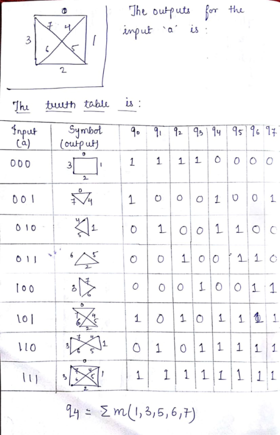
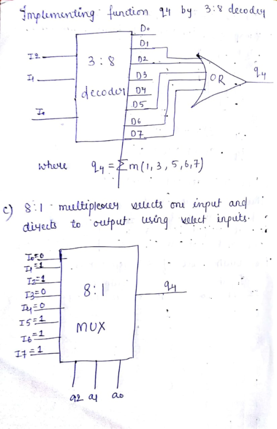
![3. [20 pts] 8-segment decoder for 8 symbols. Implement (draw logic diagram) the segment 4 of the 8-segment decoder for 8 symb](http://img.homeworklib.com/images/1e367305-8881-46ee-969a-16336ba5d38c.png?x-oss-process=image/resize,w_560)
Homework Answers

NOTE: If you are satisfied with my answer please do upvote and if
you have any kind of doubts please post in comment section. i'll
surely help you there.
Thank You:)
Add Answer to:
3. [20 pts] 8-segment decoder for 8 symbols. Implement (draw logic diagram) the segment 4 of the 8-segment decoder...
Design 3- to – 8 decoder using logic gates with enabler, AND, NOT, etc..? Design 3- to – 8 decode...
Design 3- to – 8 decoder using logic gates with enabler, AND, NOT, etc..? Design 3- to – 8 decoder using only two 2-to-4 decoders graphical blocks, use enabler input? a) Design a 3-bit ripple-carry adder using AND, OR, NOT, EXOR, etc.; include carry-in (Cin), carry-out (Cout) and overflow input/output signals? Note: Design for 1-bit first, then extrapolate to 4-bit using 1-bit full-adder graphical block. Design a 3-bit ripple-carry subtractor using AND, OR, NOT, EXOR, etc..; include carry-in (Cin), carry-out...
Truth tables of three logic functions F1, F2 and F3 given above. Implement the function F1, F2 and F3 using 3 to 8 decoder
 Q2A: Truth tables of three logic functions F1, F2 and F3 given above. Implement the function F1, F2 and F3 using 3 to 8 decoder? (Assume a 3to8 decoder component given to you, if required you may use minimum number of additional logic gates to support your design with 3 to 8 decoder) (Points) Q2B: Write HDL code to implement the above function F1, F2 and F3. All three function should include in on HDL code. In you HDL code use...
Problem 3:(10 pts) Design a synchronous machine (Transition Table, K-maps, Final Equations, Circu...
 Problem 3:(10 pts) Design a synchronous machine (Transition Table, K-maps, Final Equations, Circuit Diagram) that counts through the following sequence in the order shown below. Note, there are no inputs or output variables, so your Q values must reflect the Hex value listed B 742 D 9 3 0 and repeat a) using all D flip-flops and combinational logic (AND/OR/NOT gates only) b) using all T flip-flops and a multiplexer of size 8:1
Problem 3:(10 pts) Design a synchronous machine...
Problem 3:(10 pts) Design a synchronous machine (Transition Table, K-maps, Final Equations, Circuit Diagram) that counts through the following sequence in the order shown below. Note, there are no inputs or output variables, so your Q values must reflect the Hex value listed B 742 D 9 3 0 and repeat a) using all D flip-flops and combinational logic (AND/OR/NOT gates only) b) using all T flip-flops and a multiplexer of size 8:1
Problem 3:(10 pts) Design a synchronous machine...
1. (15 pts) Simplify the following Boolean functions using K-maps: a. F(x,y,z) = (1,4,5,6,7) b. F(x,...
 1. (15 pts) Simplify the following Boolean functions using K-maps: a. F(x,y,z) = (1,4,5,6,7) b. F(x, y, z) = (xy + xyz + xyz c. F(A,B,C,D) = 20,2,4,5,6,7,8,10,13,15) d. F(A,B,C,D) = A'B'C'D' + AB'C + B'CD' + ABCD' + BC'D e. F(A,B,C,D,E) = (0,1,4,5,16,17,21,25,29) 2. (12 pts) Consider the combinational logic circuit below and answer the following: a. Derive the Boolean expressions for Fi and F2 as functions of A, B, C, and D. b. List the complete truth table...
Design a four-bit combinational circuit 2'scomplementer. (The output generates the 2's complement of the input binary...
 Design a four-bit combinational circuit 2'scomplementer. (The output generates the 2's complement of the input binary number.) Construct a 5-to-32-line decoder with enable by using 3-to-8 and 2-to-4-line decoders with enables For the decimal-to-BCD encoder given in the text (Slide 33 of chapter 5), assume by error that the 6 input and the 3 input are both HIGH. What is the output code? Is it a valid BCD code? Construct a 16 times 1 multiplexer with 4 times 1 multiplexers....
7. Memory. A ROM chip with a size of 8 words by 4 bits is shown...
 7. Memory. A ROM chip with a size of 8 words by 4 bits is shown in the figure below. Please use this ROM chip, implement the following four logic functions by using the dot-notation. You can mark a dot to indicate that particular cell stores a value of 1. Note: in the following figure, A is the least significant bit of the address input. (10 points) F1= ABC +A C F2= ABC +BC F3= AC + B F4- ABC...
The seven-segment indicator (shown in the figure) can be used to display any of the decimal digits 0 through 9. For example "1" is displayed by lighting segment 2 and 3 and "8" by...
 The seven-segment indicator (shown in the figure) can be used to display any of the decimal digits 0 through 9. For example "1" is displayed by lighting segment 2 and 3 and "8" by lighting all seven segments. A segment is lighted when logic 1 is applied to the corresponding input on the display module. Circuit to be aputs From Switche l p Designed Design an excess-3 code convertor to derive a seven segment indicator. The four inputs to the...
ECE 1552- Summer 2019 Homework 2: Solve all questions. HW is to be turned in as a PDF or word document on canvas. Show...
 ECE 1552- Summer 2019 Homework 2: Solve all questions. HW is to be turned in as a PDF or word document on canvas. Show all working. Answers provided should be typed or written CLEARLY 1: Find a function to detect an error in the representation of a decimal digit in BCD. In other words, write an equation with value 1 when the inputs are any one of the six unused bit combinations in the BCD code, and value 0 otherwise...
·20) |19) 118) 117) 116) 115) Question 1.(20 points, I point each. Put answers into the...
 ·20) |19) 118) 117) 116) 115) Question 1.(20 points, I point each. Put answers into the above table) 13)一114) 2)- ) S-bit signed binary data can represent the decimal values from 0 to 256 2) 10111 is the two's complement representation of b. False a. True a. -23 b.-9 c.-7 d. +22 e.+7 3) 01110 is the two's complement representation of a.-13 b.-15 c.-9 d.+14 e.+18 a.A. b, B, c.A+B d, B c, (AB). a. Trueb. False a. True a....
You will use Quartus II to build an 8 bit arithmetic logic unit that performs the...
You will use Quartus II to build an 8 bit arithmetic logic unit that performs the following functions: Control Value Function 000 Copy In1 to theResult unchanged 001 Copy In2 to theResult unchanged 010 Add In1 to In2 011 Subtract In2 from In1 100 And In1 and In2 101 Or In1 and In2 110 Shift left In1 by 1 bit 111 Shift right In1 by 1 bit You are allowed to use either gates/logic schematic, or else Verilog. We suggest...
 Q2A: Truth tables of three logic functions F1, F2 and F3 given above. Implement the function F1, F2 and F3 using 3 to 8 decoder? (Assume a 3to8 decoder component given to you, if required you may use minimum number of additional logic gates to support your design with 3 to 8 decoder) (Points) Q2B: Write HDL code to implement the above function F1, F2 and F3. All three function should include in on HDL code. In you HDL code use...
 Problem 3:(10 pts) Design a synchronous machine (Transition Table, K-maps, Final Equations, Circuit Diagram) that counts through the following sequence in the order shown below. Note, there are no inputs or output variables, so your Q values must reflect the Hex value listed B 742 D 9 3 0 and repeat a) using all D flip-flops and combinational logic (AND/OR/NOT gates only) b) using all T flip-flops and a multiplexer of size 8:1
Problem 3:(10 pts) Design a synchronous machine...
Problem 3:(10 pts) Design a synchronous machine (Transition Table, K-maps, Final Equations, Circuit Diagram) that counts through the following sequence in the order shown below. Note, there are no inputs or output variables, so your Q values must reflect the Hex value listed B 742 D 9 3 0 and repeat a) using all D flip-flops and combinational logic (AND/OR/NOT gates only) b) using all T flip-flops and a multiplexer of size 8:1
Problem 3:(10 pts) Design a synchronous machine...
 1. (15 pts) Simplify the following Boolean functions using K-maps: a. F(x,y,z) = (1,4,5,6,7) b. F(x, y, z) = (xy + xyz + xyz c. F(A,B,C,D) = 20,2,4,5,6,7,8,10,13,15) d. F(A,B,C,D) = A'B'C'D' + AB'C + B'CD' + ABCD' + BC'D e. F(A,B,C,D,E) = (0,1,4,5,16,17,21,25,29) 2. (12 pts) Consider the combinational logic circuit below and answer the following: a. Derive the Boolean expressions for Fi and F2 as functions of A, B, C, and D. b. List the complete truth table...
 Design a four-bit combinational circuit 2'scomplementer. (The output generates the 2's complement of the input binary number.) Construct a 5-to-32-line decoder with enable by using 3-to-8 and 2-to-4-line decoders with enables For the decimal-to-BCD encoder given in the text (Slide 33 of chapter 5), assume by error that the 6 input and the 3 input are both HIGH. What is the output code? Is it a valid BCD code? Construct a 16 times 1 multiplexer with 4 times 1 multiplexers....
 7. Memory. A ROM chip with a size of 8 words by 4 bits is shown in the figure below. Please use this ROM chip, implement the following four logic functions by using the dot-notation. You can mark a dot to indicate that particular cell stores a value of 1. Note: in the following figure, A is the least significant bit of the address input. (10 points) F1= ABC +A C F2= ABC +BC F3= AC + B F4- ABC...
 The seven-segment indicator (shown in the figure) can be used to display any of the decimal digits 0 through 9. For example "1" is displayed by lighting segment 2 and 3 and "8" by lighting all seven segments. A segment is lighted when logic 1 is applied to the corresponding input on the display module. Circuit to be aputs From Switche l p Designed Design an excess-3 code convertor to derive a seven segment indicator. The four inputs to the...
 ECE 1552- Summer 2019 Homework 2: Solve all questions. HW is to be turned in as a PDF or word document on canvas. Show all working. Answers provided should be typed or written CLEARLY 1: Find a function to detect an error in the representation of a decimal digit in BCD. In other words, write an equation with value 1 when the inputs are any one of the six unused bit combinations in the BCD code, and value 0 otherwise...
 ·20) |19) 118) 117) 116) 115) Question 1.(20 points, I point each. Put answers into the above table) 13)一114) 2)- ) S-bit signed binary data can represent the decimal values from 0 to 256 2) 10111 is the two's complement representation of b. False a. True a. -23 b.-9 c.-7 d. +22 e.+7 3) 01110 is the two's complement representation of a.-13 b.-15 c.-9 d.+14 e.+18 a.A. b, B, c.A+B d, B c, (AB). a. Trueb. False a. True a....
Most questions answered within 3 hours.
-
HELP WITH SAS
Run the following DATA step to create a SAS data set called
ABC_CORP....
asked 6 minutes ago -
A researcher wishes to study the cumulative effects of several
combinations of HIV drugs. There are...
asked 25 minutes ago -
How
to make a simple game of whack a mole in pygame
asked 9 minutes ago -
Write a c/c++ program to read a list of students from a file and
create a...
asked 18 minutes ago -
Identify two different methods for collecting data in
qualitative research. What are the benefits and challenges...
asked 19 minutes ago -
I am suppose to have my array before the main class but I am
getting the...
asked 20 minutes ago -
Your task is to design the page table for the 32bit Pentium
microprocessor. Answer the following...
asked 27 minutes ago -
The Paradise Shoes Company has estimated its weekly TVC function
from data collected over the past...
asked 25 minutes ago -
Although Epicurus advocates pursuing pleasure for the
good life, discuss a few reasons why he does...
asked 43 minutes ago -
Problem 1: Present entries to record the selected transactions
described below:
(a)
Issued $2,790,000 of 5-year,...
asked 49 minutes ago -
Using technology to support HR activities increases:
a.
the efficiency of the administrative HR functions.
b....
asked 50 minutes ago -
1. List the features used to classify leaf
types.
2. List some characteristics that are shared...
asked 55 minutes ago