
Homework Answers
![102 {560 e figuse (aCiruit diode is severse biased because Anode of diode is ] connected to 50 through 1002 Resistance and ca](http://img.homeworklib.com/questions/a62528b0-9436-11ea-9dcd-79fdf24f82a0.png?x-oss-process=image/resize,w_560)


Add Answer to:
5. Determine whether each silicon diode in Figure 2-92 is forward-biased or reverse-biased. 6. Determine the...
ELTR 197 Analog Determine whether each silicon diode is forward or reverse biased. a) 1. b)...
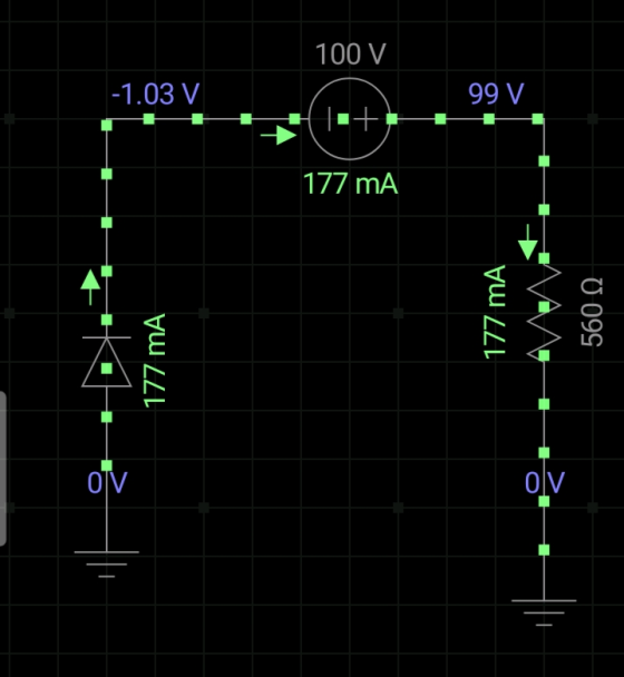
 ELTR 197 Analog Determine whether each silicon diode is forward or reverse biased. a) 1. b) 10ka 100V B) Forward Bia sE OForwod Biase 5600 5V 8V d) 10KO 10ka 1.0kn $1.5kn -20V 10V -30V 4.7ka 4.7kQ 2. Using the practical diode model, determine the values of VR1, Vr2, and Vo. Vo R1 4 k7 D1 hika 22KS) R2 10V Via- 5V 13 -n the forward current of a diode with 1. Determine whether each silicon diode is forward or...
B. In each of the following circuits: [2 marks] Determine whether each silicon diode is forward...
 B. In each of the following circuits: [2 marks] Determine
whether each silicon diode is forward biased or reverse
biased
2 A vertical plate with a gap of 2.8 cm wide of infinite extent contains a fluid of viscosity 30 poise and specific gravity 0.8. A metallic plate 1.4 mx1.4 mx0.4 cm is to be lifted up with a constant velocity of 0.18 m/sec through the gap. If the plate is in the middle of the gap. Find the force...
B. In each of the following circuits: [2 marks] Determine
whether each silicon diode is forward biased or reverse
biased
2 A vertical plate with a gap of 2.8 cm wide of infinite extent contains a fluid of viscosity 30 poise and specific gravity 0.8. A metallic plate 1.4 mx1.4 mx0.4 cm is to be lifted up with a constant velocity of 0.18 m/sec through the gap. If the plate is in the middle of the gap. Find the force...
nsider the circult shown on the right. a) Which diodes are forward biased and which are...
 nsider the circult shown on the right. a) Which diodes are forward biased and which are reverse biased? b) Assume 0.7 V drop across each forward- D1 -5V biased diode and find Vo. +5V D2 Vo +5VD3 -5V D4 Two ideal diodes are placed in a circuit shown on the 2. D1 120 D2 60 Va right: a) Determine which diodes conduct and which R 18 5.4V 5V ones do not b) Assume D1 and D2 both conduct. Find Va...
2. Sketch Vout VS Vin and Vout if Vin-10sin(2TT60t) for each of the following circuits. You may a...
 2. Sketch Vout VS Vin and Vout if Vin-10sin(2TT60t) for each of the following circuits. You may assume that the forward diode drops for the diodes equals zero Vout s v out Vin 5 V Vout out 3. Repeat problem 2 but with forward diode drops equal to 0.7 V 4. What are the primary mechanisms for current flow in a. A forward biased diode. b. A reverse biased diode not in breakdown. c. A reverse biased diode in breakdown...
3. A silicon npn bipolar transistor is uniformly doped and biased in the forward active region wi...
 3. A silicon npn bipolar transistor is uniformly doped and biased in the forward active region with the base-collector junction reverse biased by 2.5 V. The metallurgical base width is 1.5 μm. The emitter, base collector doping concentrations are 5 × 10¹⁷, 1016, 2 × 1015 cm-3 respectively. a. At T-300 K, calculate the base-emitter voltage at which the minority carrier electron concentration at x-0 is 20% of the majority carrier hole concentration. At this voltage calculate the minority carrier...
1. a) State the diode equation and explain the significance of each term. b) Sketch the current - voltage characteristics for a typical silicon diode over the 4 voltage range -2 V to +2 V. Explai...
 1. a) State the diode equation and explain the significance of each term. b) Sketch the current - voltage characteristics for a typical silicon diode over the 4 voltage range -2 V to +2 V. Explain how the characteristics would change if the diode was fabricated using germanium. Give an equivalent circuit representation of the device in each case. c) In a silicon diode a current of 200 HA flows when a forward bias voltage of 0.5 V4 is applied...
For the double diode circuit shown in figure 2-1, answer the following questions. In Figure 2-1...
 For the double diode circuit shown in figure 2-1, answer the following questions. In Figure 2-1 a) (10pts) For the triangular wave input shown (Vin), sketch the output voltage (Vout) using the constant voltage drop model (CVD: Vo-0.7V). Be sure to note the voltage values on the y-axis of your Vout plot and show any equations you used to determine those values ime FEE 334: Spring 2019 Midterm b) (2pts) During the middle of the first time segment (when Vin...
The silicon diode shown in the given figure is described by ip = I. (ed/- 1)...
 The silicon diode shown in the given figure is described by ip = I. (ed/- 1) where at T = 300 K, 1. = 250 x 10-12 A, VT = KT 26 mV, vs = Vs + V3 = 4.2V + 110 cos(wt) mV,w = 377 rad/s, and R = 10 ko. The DC operating (quiescent) point Q and the AC small-signal equivalent resistance at Q are as follows: IDQ = 0.548 mA, VDQ = 0.365 V, and ra =...
Ctri Question 3 (20 Marks) Lab 1-Zener Circuits and Applications Theory: Zener diode is designed ...
 Ctri Question 3 (20 Marks) Lab 1-Zener Circuits and Applications Theory: Zener diode is designed to operate in reverse conduction. Zener breakdown occurs at a precisely defined voltage, allowing the diode to be used as a voltage reference or clipper. While Zener diodes are usually operated in reverse conduction, they may also be operated in cutoff and forward conduction. There are two different effects that are used in "Zener diodes". The only practical difference is that the two types have...
consider a silicon pn junction diode at 300 K with nd= na = 10^16 cm-3, u_n 1350 cm^2/v-s, u_p 480 cm^2/v-s, and t_no = t_po= 5×10^-7 s. consider two bias conditions: i) a reverse bias of 1.0 v ii) a...
consider a silicon pn junction diode at 300 K with nd= na = 10^16 cm-3, u_n 1350 cm^2/v-s, u_p 480 cm^2/v-s, and t_no = t_po= 5×10^-7 s. consider two bias conditions: i) a reverse bias of 1.0 v ii) a forward bias of 0.2 v a) for each bus condition, roughly sketch the band gap diagram - accurately label the energy gap in eV - indicate the difference between E_f on the two sides id the junction and label its...
 ELTR 197 Analog Determine whether each silicon diode is forward or reverse biased. a) 1. b) 10ka 100V B) Forward Bia sE OForwod Biase 5600 5V 8V d) 10KO 10ka 1.0kn $1.5kn -20V 10V -30V 4.7ka 4.7kQ 2. Using the practical diode model, determine the values of VR1, Vr2, and Vo. Vo R1 4 k7 D1 hika 22KS) R2 10V Via- 5V 13 -n the forward current of a diode with 1. Determine whether each silicon diode is forward or...
 B. In each of the following circuits: [2 marks] Determine
whether each silicon diode is forward biased or reverse
biased
2 A vertical plate with a gap of 2.8 cm wide of infinite extent contains a fluid of viscosity 30 poise and specific gravity 0.8. A metallic plate 1.4 mx1.4 mx0.4 cm is to be lifted up with a constant velocity of 0.18 m/sec through the gap. If the plate is in the middle of the gap. Find the force...
B. In each of the following circuits: [2 marks] Determine
whether each silicon diode is forward biased or reverse
biased
2 A vertical plate with a gap of 2.8 cm wide of infinite extent contains a fluid of viscosity 30 poise and specific gravity 0.8. A metallic plate 1.4 mx1.4 mx0.4 cm is to be lifted up with a constant velocity of 0.18 m/sec through the gap. If the plate is in the middle of the gap. Find the force...
 nsider the circult shown on the right. a) Which diodes are forward biased and which are reverse biased? b) Assume 0.7 V drop across each forward- D1 -5V biased diode and find Vo. +5V D2 Vo +5VD3 -5V D4 Two ideal diodes are placed in a circuit shown on the 2. D1 120 D2 60 Va right: a) Determine which diodes conduct and which R 18 5.4V 5V ones do not b) Assume D1 and D2 both conduct. Find Va...
 2. Sketch Vout VS Vin and Vout if Vin-10sin(2TT60t) for each of the following circuits. You may assume that the forward diode drops for the diodes equals zero Vout s v out Vin 5 V Vout out 3. Repeat problem 2 but with forward diode drops equal to 0.7 V 4. What are the primary mechanisms for current flow in a. A forward biased diode. b. A reverse biased diode not in breakdown. c. A reverse biased diode in breakdown...
 3. A silicon npn bipolar transistor is uniformly doped and biased in the forward active region with the base-collector junction reverse biased by 2.5 V. The metallurgical base width is 1.5 μm. The emitter, base collector doping concentrations are 5 × 10¹⁷, 1016, 2 × 1015 cm-3 respectively. a. At T-300 K, calculate the base-emitter voltage at which the minority carrier electron concentration at x-0 is 20% of the majority carrier hole concentration. At this voltage calculate the minority carrier...
 1. a) State the diode equation and explain the significance of each term. b) Sketch the current - voltage characteristics for a typical silicon diode over the 4 voltage range -2 V to +2 V. Explain how the characteristics would change if the diode was fabricated using germanium. Give an equivalent circuit representation of the device in each case. c) In a silicon diode a current of 200 HA flows when a forward bias voltage of 0.5 V4 is applied...
 For the double diode circuit shown in figure 2-1, answer the following questions. In Figure 2-1 a) (10pts) For the triangular wave input shown (Vin), sketch the output voltage (Vout) using the constant voltage drop model (CVD: Vo-0.7V). Be sure to note the voltage values on the y-axis of your Vout plot and show any equations you used to determine those values ime FEE 334: Spring 2019 Midterm b) (2pts) During the middle of the first time segment (when Vin...
 The silicon diode shown in the given figure is described by ip = I. (ed/- 1) where at T = 300 K, 1. = 250 x 10-12 A, VT = KT 26 mV, vs = Vs + V3 = 4.2V + 110 cos(wt) mV,w = 377 rad/s, and R = 10 ko. The DC operating (quiescent) point Q and the AC small-signal equivalent resistance at Q are as follows: IDQ = 0.548 mA, VDQ = 0.365 V, and ra =...
 Ctri Question 3 (20 Marks) Lab 1-Zener Circuits and Applications Theory: Zener diode is designed to operate in reverse conduction. Zener breakdown occurs at a precisely defined voltage, allowing the diode to be used as a voltage reference or clipper. While Zener diodes are usually operated in reverse conduction, they may also be operated in cutoff and forward conduction. There are two different effects that are used in "Zener diodes". The only practical difference is that the two types have...
Most questions answered within 3 hours.
-
Le Terroir Winery is considering an expansion project to produce
fine wines. The trial expansion will...
asked 2 minutes ago -
The Bahraini public budget experiences deficit in the last
seven years, what are procedures are taken...
asked 9 minutes ago -
You invested $30,000 in a mutual fund at the beginning of the
year when the NAV...
asked 13 minutes ago -
Would you expect the price elasticity of supply for guitars to
be more inelastic in the...
asked 15 minutes ago -
A snowmobile is originally at the point with position vector
30.1 m at 95.0° counterclockwise from...
asked 15 minutes ago -
MAN3240 Organizational Behavior
In one to two paragraphs
6.) How can understanding emotions make me more...
asked 23 minutes ago -
Identify one individual who, in your opinion, is an excellent
leader. List the qualities that this...
asked 20 minutes ago -
For the data set shown below, complete parts (a) through (d)
below. x 3 4 5...
asked 26 minutes ago -
A university administrator working in student housing wants to
determine if the percentage of students residing...
asked 40 minutes ago -
3). Describe human population growth that has occurred in the
past 400 years. Use terms learned...
asked 37 minutes ago -
A
projectile is blue at a target. The distance from the point of
impact to the...
asked 1 hour ago -
Given a 32 bit processor, with 2 MB of physical RAM split into 512
frames. What...
asked 52 minutes ago