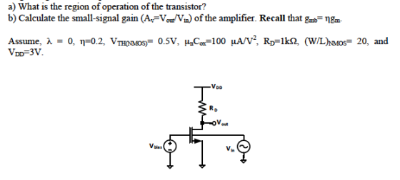
It is possible to use the bulk terminal of a transistor as an input of an amplifier. Consider the single-stage NMOS amplifier shown below.

Homework Answers
Request Answer!
We need at least 10 more requests to produce the answer.
0 / 10 have requested this problem solution
The more requests, the faster the answer.
Add Answer to:
It is possible to use the bulk terminal of a transistor as an
input of an...
In the amplifier circuit below, the transistor has the following properties:Vt =1.5V,k’n=100 microA/V2,W=2 micro m ,L=0.2...
 In the amplifier circuit below, the transistor has the following
properties:Vt =1.5V,k’n=100 microA/V2,W=2 micro m ,L=0.2 micro m,
lambda = 0V^-1
a. Find the dc values VG, VD, and VS.
b. Verify (prove) that the circuit is in the proper region of
operation for an amplifier
c. Find the transconductance value, gm
d. Draw the equivalent small-signal circuit model, replacing the
NMOS with its pi-model
e. Draw the equivalent small-signal circuit model, replacing the
NMOS with its T-model
f. Calculate...
In the amplifier circuit below, the transistor has the following
properties:Vt =1.5V,k’n=100 microA/V2,W=2 micro m ,L=0.2 micro m,
lambda = 0V^-1
a. Find the dc values VG, VD, and VS.
b. Verify (prove) that the circuit is in the proper region of
operation for an amplifier
c. Find the transconductance value, gm
d. Draw the equivalent small-signal circuit model, replacing the
NMOS with its pi-model
e. Draw the equivalent small-signal circuit model, replacing the
NMOS with its T-model
f. Calculate...
Capacitor values can be assumed to be large enough in the small-signal analysis frequency band. (Hint:...
 Capacitor values can be assumed to be large enough in the
small-signal analysis frequency band. (Hint: Consider separating
the bias and small-signal signals.) 1. Find the bias current
flowing into the transistor (λ=0) 2. Find the small-signal voltage
gain Vout/Vin value. (λ=0.1V^(-1))
Vpp=20V T VBias=3V Rp=10k Rg=90k 2 Vout VIN - HE Rsig=10812 B=1mA/V2 Vth=1V Rs=50012
Capacitor values can be assumed to be large enough in the
small-signal analysis frequency band. (Hint: Consider separating
the bias and small-signal signals.) 1. Find the bias current
flowing into the transistor (λ=0) 2. Find the small-signal voltage
gain Vout/Vin value. (λ=0.1V^(-1))
Vpp=20V T VBias=3V Rp=10k Rg=90k 2 Vout VIN - HE Rsig=10812 B=1mA/V2 Vth=1V Rs=50012
A MOSFET is wired as a common-source amplifier as shown below. The input voltage vIN is...
 A MOSFET is wired as a common-source amplifier as shown below.
The input voltage vIN is the total of the source for
biasing the circuit at its operating point (vBIAS), and
a small signal ac source providing the signal that we want to
amplify (vin). The total output voltage is
vO.
a) Assume VDD = 5?, VIN = 2?, and ? = 4?Ω
in the circuit and the MOSFET parameters are K =
0.5??/?2, VTH 1?, and ? = 0.05V-1....
A MOSFET is wired as a common-source amplifier as shown below.
The input voltage vIN is the total of the source for
biasing the circuit at its operating point (vBIAS), and
a small signal ac source providing the signal that we want to
amplify (vin). The total output voltage is
vO.
a) Assume VDD = 5?, VIN = 2?, and ? = 4?Ω
in the circuit and the MOSFET parameters are K =
0.5??/?2, VTH 1?, and ? = 0.05V-1....
QUESTION (1) Transistor Mi in this common base amplifier circuit has the following characteristics: +Vc VTH...
 QUESTION (1) Transistor Mi in this common base amplifier circuit has the following characteristics: +Vc VTH =1 V Rp R, C. K 1 mA/V2 2 0.1 R Given: Vcc 2 mA, 10 V, lbias Ct C2 0, 5 k2, RD 2 k2 RI 10 k, R2 R (12 points) a) Determine the small signal gain, vo/Vin. (4 points) b) Determine the input resistance, Rin. (4 points) c) Determine the output resistance, Ro. Useful formulae: for n-channel MOSFET triode region =...
Exercise 12.13 Derive expressions for the voltage gain, input resistance, and output resistance of the common-gate...
 Exercise 12.13 Derive expressions for the voltage gain, input resistance, and output resistance of the common-gate amplifier shown in Figure 12.29, assuming that ra is an open circuit Answer The small-signal equivalent circuit is shown in Figure 12.30. A Rin 1/(gm 1/Rs); Ro = Rp. gmR/; +VDD С2 + RL Vo CL R + Vin v(t) -Vss W Ri Rp R 8mVgs Vo Rs Vin + v(t)
Exercise 12.13 Derive expressions for the voltage gain, input resistance, and output resistance...
Exercise 12.13 Derive expressions for the voltage gain, input resistance, and output resistance of the common-gate amplifier shown in Figure 12.29, assuming that ra is an open circuit Answer The small-signal equivalent circuit is shown in Figure 12.30. A Rin 1/(gm 1/Rs); Ro = Rp. gmR/; +VDD С2 + RL Vo CL R + Vin v(t) -Vss W Ri Rp R 8mVgs Vo Rs Vin + v(t)
Exercise 12.13 Derive expressions for the voltage gain, input resistance, and output resistance...
URGENT The NMOS in the shown figure has Vt = 0.8V, kn = 5 mA/V2, and...
 URGENT
The NMOS in the shown figure has Vt = 0.8V, kn = 5 mA/V2, and VA = 40 V. The circuit also has Vdd = 5V, VSS = -5V, RG = RLD = 1 M2, and RLS = 0 A. [3 marks] Neglecting the channel length modulation effect, find the value of Rs so that the NMOS operates in saturation with Ip = 0.4 mA B. [2 marks] Neglecting the channel length modulation effect, find the largest possible value...
URGENT
The NMOS in the shown figure has Vt = 0.8V, kn = 5 mA/V2, and VA = 40 V. The circuit also has Vdd = 5V, VSS = -5V, RG = RLD = 1 M2, and RLS = 0 A. [3 marks] Neglecting the channel length modulation effect, find the value of Rs so that the NMOS operates in saturation with Ip = 0.4 mA B. [2 marks] Neglecting the channel length modulation effect, find the largest possible value...
In the CE amplifier shown below, a. Find the transistor DC operating points. Check what region...
 In the CE amplifier shown below, a. Find the transistor DC operating points. Check what region of operation the transistor is biased at. b. Calculate the small signal voltage gain, the input resistance looking into the base of the transistor, and the output resistance looking down at the collector. c. Find the small signal current gain, 으 VBE,ON = 0.6V, and β = 100, VA = 00, Base current may be ignored if possible
1 bias V. out 2 2:1 mirror 6:52 PMw Variahle 2:1 mirror S Transistor PMOS Transistor Variable NMO 1 00 0.5 0.10 35 0.5 0.20 VT (V) A (1M) L (um) Vdd is 3V The bias current is 40μΑ the bias voltag...
 1 bias V. out 2 2:1 mirror 6:52 PMw Variahle 2:1 mirror S Transistor PMOS Transistor Variable NMO 1 00 0.5 0.10 35 0.5 0.20 VT (V) A (1M) L (um) Vdd is 3V The bias current is 40μΑ the bias voltage at the rot. Vin-is2.8V, and thie voltage ut port a is O.7V. The load capacitance (CL) is Sp The NMOS current mirror is 2:1 NOTE: All 3 devices are NMOS above Include proper units for full credit and...
1. Consider NMOS transistor in the circuit that has u.Cox = 0.4 mA/V?, W/L = 25,...
 1. Consider NMOS transistor in the circuit that has u.Cox = 0.4 mA/V?, W/L = 25, and V.=0.4V. (20 pts) (a) Find the value of Vas that results in saturation mode operation with a lp current of 0.1 mA. Neglect the Early effect. (2.5 pts) +1.5 V in BRD (b) Find the value of Rp that results in a de drain voltage of 0.5V. (2.5 pts) = = = (e) Find gw and r, at the de operating point specified...
3. In Figure 3 on page 5, the DC operating point for the PNP transistor Qi...
 3. In Figure 3 on page 5, the DC operating point for the PNP transistor Qi is Ic = 0.33 mA and Vec = 2.4 V, and the DC operating point for the NMOS transistor Mi is ID = 2.81 mA and Vos = 2.92 V. Qı has B = 100, VA = 85 V at room temperature and Mi has Kn= 1 mA/V2, Vin= 1 V and 2 = 0.02 V-1. Assume that the capacitors have infinite values, and...
 In the amplifier circuit below, the transistor has the following
properties:Vt =1.5V,k’n=100 microA/V2,W=2 micro m ,L=0.2 micro m,
lambda = 0V^-1
a. Find the dc values VG, VD, and VS.
b. Verify (prove) that the circuit is in the proper region of
operation for an amplifier
c. Find the transconductance value, gm
d. Draw the equivalent small-signal circuit model, replacing the
NMOS with its pi-model
e. Draw the equivalent small-signal circuit model, replacing the
NMOS with its T-model
f. Calculate...
In the amplifier circuit below, the transistor has the following
properties:Vt =1.5V,k’n=100 microA/V2,W=2 micro m ,L=0.2 micro m,
lambda = 0V^-1
a. Find the dc values VG, VD, and VS.
b. Verify (prove) that the circuit is in the proper region of
operation for an amplifier
c. Find the transconductance value, gm
d. Draw the equivalent small-signal circuit model, replacing the
NMOS with its pi-model
e. Draw the equivalent small-signal circuit model, replacing the
NMOS with its T-model
f. Calculate...
 Capacitor values can be assumed to be large enough in the
small-signal analysis frequency band. (Hint: Consider separating
the bias and small-signal signals.) 1. Find the bias current
flowing into the transistor (λ=0) 2. Find the small-signal voltage
gain Vout/Vin value. (λ=0.1V^(-1))
Vpp=20V T VBias=3V Rp=10k Rg=90k 2 Vout VIN - HE Rsig=10812 B=1mA/V2 Vth=1V Rs=50012
Capacitor values can be assumed to be large enough in the
small-signal analysis frequency band. (Hint: Consider separating
the bias and small-signal signals.) 1. Find the bias current
flowing into the transistor (λ=0) 2. Find the small-signal voltage
gain Vout/Vin value. (λ=0.1V^(-1))
Vpp=20V T VBias=3V Rp=10k Rg=90k 2 Vout VIN - HE Rsig=10812 B=1mA/V2 Vth=1V Rs=50012
 A MOSFET is wired as a common-source amplifier as shown below.
The input voltage vIN is the total of the source for
biasing the circuit at its operating point (vBIAS), and
a small signal ac source providing the signal that we want to
amplify (vin). The total output voltage is
vO.
a) Assume VDD = 5?, VIN = 2?, and ? = 4?Ω
in the circuit and the MOSFET parameters are K =
0.5??/?2, VTH 1?, and ? = 0.05V-1....
A MOSFET is wired as a common-source amplifier as shown below.
The input voltage vIN is the total of the source for
biasing the circuit at its operating point (vBIAS), and
a small signal ac source providing the signal that we want to
amplify (vin). The total output voltage is
vO.
a) Assume VDD = 5?, VIN = 2?, and ? = 4?Ω
in the circuit and the MOSFET parameters are K =
0.5??/?2, VTH 1?, and ? = 0.05V-1....
 QUESTION (1) Transistor Mi in this common base amplifier circuit has the following characteristics: +Vc VTH =1 V Rp R, C. K 1 mA/V2 2 0.1 R Given: Vcc 2 mA, 10 V, lbias Ct C2 0, 5 k2, RD 2 k2 RI 10 k, R2 R (12 points) a) Determine the small signal gain, vo/Vin. (4 points) b) Determine the input resistance, Rin. (4 points) c) Determine the output resistance, Ro. Useful formulae: for n-channel MOSFET triode region =...
 Exercise 12.13 Derive expressions for the voltage gain, input resistance, and output resistance of the common-gate amplifier shown in Figure 12.29, assuming that ra is an open circuit Answer The small-signal equivalent circuit is shown in Figure 12.30. A Rin 1/(gm 1/Rs); Ro = Rp. gmR/; +VDD С2 + RL Vo CL R + Vin v(t) -Vss W Ri Rp R 8mVgs Vo Rs Vin + v(t)
Exercise 12.13 Derive expressions for the voltage gain, input resistance, and output resistance...
Exercise 12.13 Derive expressions for the voltage gain, input resistance, and output resistance of the common-gate amplifier shown in Figure 12.29, assuming that ra is an open circuit Answer The small-signal equivalent circuit is shown in Figure 12.30. A Rin 1/(gm 1/Rs); Ro = Rp. gmR/; +VDD С2 + RL Vo CL R + Vin v(t) -Vss W Ri Rp R 8mVgs Vo Rs Vin + v(t)
Exercise 12.13 Derive expressions for the voltage gain, input resistance, and output resistance...
 URGENT
The NMOS in the shown figure has Vt = 0.8V, kn = 5 mA/V2, and VA = 40 V. The circuit also has Vdd = 5V, VSS = -5V, RG = RLD = 1 M2, and RLS = 0 A. [3 marks] Neglecting the channel length modulation effect, find the value of Rs so that the NMOS operates in saturation with Ip = 0.4 mA B. [2 marks] Neglecting the channel length modulation effect, find the largest possible value...
URGENT
The NMOS in the shown figure has Vt = 0.8V, kn = 5 mA/V2, and VA = 40 V. The circuit also has Vdd = 5V, VSS = -5V, RG = RLD = 1 M2, and RLS = 0 A. [3 marks] Neglecting the channel length modulation effect, find the value of Rs so that the NMOS operates in saturation with Ip = 0.4 mA B. [2 marks] Neglecting the channel length modulation effect, find the largest possible value...
 In the CE amplifier shown below, a. Find the transistor DC operating points. Check what region of operation the transistor is biased at. b. Calculate the small signal voltage gain, the input resistance looking into the base of the transistor, and the output resistance looking down at the collector. c. Find the small signal current gain, 으 VBE,ON = 0.6V, and β = 100, VA = 00, Base current may be ignored if possible
 1 bias V. out 2 2:1 mirror 6:52 PMw Variahle 2:1 mirror S Transistor PMOS Transistor Variable NMO 1 00 0.5 0.10 35 0.5 0.20 VT (V) A (1M) L (um) Vdd is 3V The bias current is 40μΑ the bias voltage at the rot. Vin-is2.8V, and thie voltage ut port a is O.7V. The load capacitance (CL) is Sp The NMOS current mirror is 2:1 NOTE: All 3 devices are NMOS above Include proper units for full credit and...
 1. Consider NMOS transistor in the circuit that has u.Cox = 0.4 mA/V?, W/L = 25, and V.=0.4V. (20 pts) (a) Find the value of Vas that results in saturation mode operation with a lp current of 0.1 mA. Neglect the Early effect. (2.5 pts) +1.5 V in BRD (b) Find the value of Rp that results in a de drain voltage of 0.5V. (2.5 pts) = = = (e) Find gw and r, at the de operating point specified...
 3. In Figure 3 on page 5, the DC operating point for the PNP transistor Qi is Ic = 0.33 mA and Vec = 2.4 V, and the DC operating point for the NMOS transistor Mi is ID = 2.81 mA and Vos = 2.92 V. Qı has B = 100, VA = 85 V at room temperature and Mi has Kn= 1 mA/V2, Vin= 1 V and 2 = 0.02 V-1. Assume that the capacitors have infinite values, and...
Most questions answered within 3 hours.
-
What kind of materials are found in Leviticus? Give a simple
description of this book. Also...
asked 2 minutes ago -
17.1 Energy drink commercials. A study was designed to compare
Red Bull energy drink commercials. Each...
asked 6 minutes ago -
The life that maximizes net present value and shareholder wealth
is known as...
Physical Life
Economic...
asked 30 minutes ago -
You have to write your code in C++ (as a cpp file) and prepare a
docx...
asked 1 hour ago -
Why does the spectrum of bromocresol green changes at different
pHs? What causes the change?
asked 1 hour ago -
Rice Company has a unit selling price of $690, variable costs
per unit of $390, and...
asked 2 hours ago -
The DeVille Company reported pretax accounting
income on its income statement as follows:
2018
$
425,000...
asked 2 hours ago -
Argue for or against the "Three Strikes"laws. Provide a rationale
to support your response.
asked 3 hours ago -
Bargaining Models: what is the "Obsolescing Bargain"?
Bargaining Models: what are the factors that would tend...
asked 4 hours ago -
1. A ball is thrown up into the air.
a) Draw motion diagram and the point-like...
asked 4 hours ago -
1) Because money eliminates the "double coincidence of wants"
problem, the development of money as a...
asked 4 hours ago -
Company AAA produces only one product which other manufacturers
purchase as a component for their final...
asked 7 hours ago