

Homework Answers

Add Answer to:
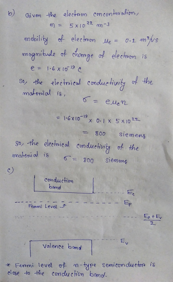
An n-type germanium specimen is known to have an electron concentration of 5 x 10²² m-?....
Please help me 1. In degenerate p-type silicon, a. The Fermi energy is above the valence...
 Please help me
1. In degenerate p-type silicon, a. The Fermi energy is above the valence energy and below the intrinsic Fermi energy b. The Fermi energy is below the valence energy c. The Fermi energy is above the conduction energy d. The Fermi energy is below the conduction energy and above the intrinsic Fermi energy 2. A semiconductor has No 5X 1010 cm3 and N-2X 1018 cm2. It is a. b. C. d. N-type and electrons are the majority...
Please help me
1. In degenerate p-type silicon, a. The Fermi energy is above the valence energy and below the intrinsic Fermi energy b. The Fermi energy is below the valence energy c. The Fermi energy is above the conduction energy d. The Fermi energy is below the conduction energy and above the intrinsic Fermi energy 2. A semiconductor has No 5X 1010 cm3 and N-2X 1018 cm2. It is a. b. C. d. N-type and electrons are the majority...
Crystal types are sometimes classified based on the type of bonding, for example ionic crystals. Name...
 Crystal types are sometimes classified based on the type of bonding, for example ionic crystals. Name two other types of crystal. (b) A crystal is formed from N atoms. Give a brief description of the origin of energy bands in solids. (c) Sketch the band structure of an undoped semiconductor, label the conduction and valence bands, and the relevant energies. Mark the position of the Fermi energy. Make a second sketch and assume the semiconductor has been doped n -...
Assume a p-n step junction in silicon wi concentration of 2x10¹⁶,c? and the n-type material doped...
 Assume a p-n step junction in silicon wi concentration of 2x10¹⁶,c? and the n-type material doped at 3X10-s,cm3 The intrinsic carrier density is 1.25X101°/cm and all dopants are fully ionized Assume that the effective density of states for silicon is 3.3x10 cm3 for the conduction band and 1.75x101 cm for the valence band. Assume that the temperature is 300K and silicon relative permittivity of 11.7 a. Compute the hole concentration on the n-side and electron concentration th the p-type material...
9. An n- type germanium semiconductor sample is brought into contact with a p - type...
 9. An n- type germanium semiconductor sample is brought into contact with a p - type silicon sample. The germanium sample has a carrier concentra- tion of 4.5 x 1016cm-3 and the silicon sample has a carrier concentration of 1.0 × 1016cm-3. At 300K the intrinsic carrier concentration of germanium is 2.4 × 1013cm-3 and its band gap is 0.66 eV. At 300K the intrinsic carrier concentration of silicon is 1.45 × 1010cm-3 and its band gap is 1.12 eV....
A piece of p-type GaAs is doped with a net impurity concentration of N Na-5 × 10¹⁸ m-3. Is it deg...
 A piece of p-type GaAs is doped with a net impurity concentration of N Na-5 × 10¹⁸ m-3. Is it degenerate or nondegenerate? Find its electron and hole concentrations and its Fermi level at 300 K. How much is the shift of the Fermi level, measured from the intrinsic Fermi level, caused by the doping of the impurity? Compare the results obtained in this problem for the p-type GaAs with those found in Example 12.3 for the n-type GaAs of...
He 17 Al Si P S CIAr 12 35 Zn Ga Ge As Se Br Kr 53 51 116 115 113 112 GaN is known as a IlI-IV intrinsic semiconductor. Ga has 3 electrons in its outermost shell, and N has 5. Ga and N share electron...
 He 17 Al Si P S CIAr 12 35 Zn Ga Ge As Se Br Kr 53 51 116 115 113 112 GaN is known as a IlI-IV intrinsic semiconductor. Ga has 3 electrons in its outermost shell, and N has 5. Ga and N share electrons so that each has 8 electrons, producing a completely full valence band What element could be a n-type dopant in GaN? You must also state which site (e.g. replacing Ga or N) the...
Taking pure silicon (Si) as an example, explain what is meant by the terms electron-hole generation...
 Taking pure silicon (Si) as an example, explain what is meant by the terms electron-hole generation and recombination, how they affect the electrical conductivity, and define what is meant by the "intrinsic carrier density", n. [5 marks] Q3. a) b) With the aid of both lattice and energy band diagrams, explain how n-type doping of Si is achieved and state two types of suitable dopant atoms. [7 marks] c) An n-type region on a Si wafer has a donor concentration...
EENG 245 Physical electronics HW 1 1) The NaCl crystal is cubic, and can be described...
 EENG 245 Physical electronics HW 1 1) The NaCl crystal is cubic, and can be described as follows. Na atoms sit at the corners and faces of a cube, and Cl atoms sit in between two Na atoms. This means that a Clatom is found half-way along each of the cube edges, and there is a Cl in the center of the cube. (We could also have described the lattice by interchanging Na and Cl in the description above.) Another...
 Please help me
1. In degenerate p-type silicon, a. The Fermi energy is above the valence energy and below the intrinsic Fermi energy b. The Fermi energy is below the valence energy c. The Fermi energy is above the conduction energy d. The Fermi energy is below the conduction energy and above the intrinsic Fermi energy 2. A semiconductor has No 5X 1010 cm3 and N-2X 1018 cm2. It is a. b. C. d. N-type and electrons are the majority...
Please help me
1. In degenerate p-type silicon, a. The Fermi energy is above the valence energy and below the intrinsic Fermi energy b. The Fermi energy is below the valence energy c. The Fermi energy is above the conduction energy d. The Fermi energy is below the conduction energy and above the intrinsic Fermi energy 2. A semiconductor has No 5X 1010 cm3 and N-2X 1018 cm2. It is a. b. C. d. N-type and electrons are the majority...
 Crystal types are sometimes classified based on the type of bonding, for example ionic crystals. Name two other types of crystal. (b) A crystal is formed from N atoms. Give a brief description of the origin of energy bands in solids. (c) Sketch the band structure of an undoped semiconductor, label the conduction and valence bands, and the relevant energies. Mark the position of the Fermi energy. Make a second sketch and assume the semiconductor has been doped n -...
 Assume a p-n step junction in silicon wi concentration of 2x10¹⁶,c? and the n-type material doped at 3X10-s,cm3 The intrinsic carrier density is 1.25X101°/cm and all dopants are fully ionized Assume that the effective density of states for silicon is 3.3x10 cm3 for the conduction band and 1.75x101 cm for the valence band. Assume that the temperature is 300K and silicon relative permittivity of 11.7 a. Compute the hole concentration on the n-side and electron concentration th the p-type material...
 9. An n- type germanium semiconductor sample is brought into contact with a p - type silicon sample. The germanium sample has a carrier concentra- tion of 4.5 x 1016cm-3 and the silicon sample has a carrier concentration of 1.0 × 1016cm-3. At 300K the intrinsic carrier concentration of germanium is 2.4 × 1013cm-3 and its band gap is 0.66 eV. At 300K the intrinsic carrier concentration of silicon is 1.45 × 1010cm-3 and its band gap is 1.12 eV....
 A piece of p-type GaAs is doped with a net impurity concentration of N Na-5 × 10¹⁸ m-3. Is it degenerate or nondegenerate? Find its electron and hole concentrations and its Fermi level at 300 K. How much is the shift of the Fermi level, measured from the intrinsic Fermi level, caused by the doping of the impurity? Compare the results obtained in this problem for the p-type GaAs with those found in Example 12.3 for the n-type GaAs of...
 He 17 Al Si P S CIAr 12 35 Zn Ga Ge As Se Br Kr 53 51 116 115 113 112 GaN is known as a IlI-IV intrinsic semiconductor. Ga has 3 electrons in its outermost shell, and N has 5. Ga and N share electrons so that each has 8 electrons, producing a completely full valence band What element could be a n-type dopant in GaN? You must also state which site (e.g. replacing Ga or N) the...
 Taking pure silicon (Si) as an example, explain what is meant by the terms electron-hole generation and recombination, how they affect the electrical conductivity, and define what is meant by the "intrinsic carrier density", n. [5 marks] Q3. a) b) With the aid of both lattice and energy band diagrams, explain how n-type doping of Si is achieved and state two types of suitable dopant atoms. [7 marks] c) An n-type region on a Si wafer has a donor concentration...
 EENG 245 Physical electronics HW 1 1) The NaCl crystal is cubic, and can be described as follows. Na atoms sit at the corners and faces of a cube, and Cl atoms sit in between two Na atoms. This means that a Clatom is found half-way along each of the cube edges, and there is a Cl in the center of the cube. (We could also have described the lattice by interchanging Na and Cl in the description above.) Another...
Most questions answered within 3 hours.
-
The blues made its way into many kinds of music. Eric Clapton,
The Beatles, and Elvis...
asked 53 minutes ago -
If you’re standing at the bottom of a hill and asked to evaluate
it while being...
asked 1 hour ago -
1. Which region has taken the lead in the world of
e-waste handling?
a) European Union...
asked 1 hour ago -
A 8.15- g bullet from a 9-mm pistol has a velocity of 366.0 m/s.
It strikes...
asked 3 hours ago -
The outstanding bonds of Alpha Extracts have a yield to maturity
of 7.4 percent and a...
asked 3 hours ago -
The Problem: The Case of the Harmonizing Vacations
Your CEO is exploring partnering with a European...
asked 4 hours ago -
A chemical equation is balanced by adding coefficients in front
of some formulas so that the...
asked 4 hours ago -
From the literature (reference your sources): What are the
lattice parameters of calcite and aragonite? Why...
asked 5 hours ago -
Your system is rejecting the question am asking which is
preceded by a case study. It...
asked 5 hours ago -
3. On January 2, 2000, Larry creates a trust with himself as
trustee. Larry as trustee...
asked 5 hours ago -
A member of the volleyball team spikes the ball. During this
process, she changes the velocity...
asked 5 hours ago -
Are adult gamers less likely to use a gaming console (Xbox,
PlayStation, Wii, etc...) than teen...
asked 6 hours ago