
Homework Answers
Add Answer to:
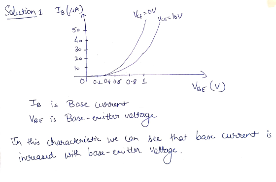
1) Plot base current of a npn transistor versus base-emitter voltage 2) Plot Gate current of...
Consider a silicon device (which happens to be an npn bipolar transistor) with an emitter doping...
Consider a silicon device (which happens to be an npn bipolar transistor) with an emitter doping of 10^17/cm3, a base doping of 8x10^15/cm3 and a collector doping of 2x10^15/cm3. Carefully calculate how the band diagram, charge density, electric field and electrostatic potential as a function of distance for this device changes from the equilibrium case when this bipolar transistor is properly biased to work as an amplifier. In other words, show how the band diagram changes when the emitter-base junction...
2. (15 pts) An npn bipolar junction transistor is biased in the forward-active region. The common-base...
 2. (15 pts) An npn bipolar junction transistor is biased in the forward-active region. The common-base current gain, α 0.95. The input emitter current is IE-4.6 mA. a) Calculate the collector current Ic b) Calculate the common-emitter current gain, B c) Calculate the base current IB IB
2. Consider an N-channel MOSFET circuit where the gate and drain terminals are shorted to- gether...
 Please help, and explain as much as possible. Thank
you!
2. Consider an N-channel MOSFET circuit where the gate and drain terminals are shorted to- gether2 as shown in Figre 2. Assume that the MOSFET has trans-conductance parameter of gm = 0.5mA/V and the threshold voltage of 0.7V (a) Identify in which region the n-channel MOSFET is operating (Triode region or Saturation region)? (b) Write MATLAB code to compute the drain current for the following gate-to-source voltage, Vcs Ves-VDs 0,1,2,3,4,5,6,7...
Please help, and explain as much as possible. Thank
you!
2. Consider an N-channel MOSFET circuit where the gate and drain terminals are shorted to- gether2 as shown in Figre 2. Assume that the MOSFET has trans-conductance parameter of gm = 0.5mA/V and the threshold voltage of 0.7V (a) Identify in which region the n-channel MOSFET is operating (Triode region or Saturation region)? (b) Write MATLAB code to compute the drain current for the following gate-to-source voltage, Vcs Ves-VDs 0,1,2,3,4,5,6,7...
Problem 2. A silicon NPN bipolar transistor has the following specifications: Emitter: N+: ND =1018 cm-3...
Problem 2. A silicon NPN bipolar transistor has the following specifications: Emitter: N+: ND =1018 cm-3 , base: p-type, NA=1015 cm-3, collector: N-type, ND=5x1015 cm-3 . 1. Draw the energy band diagram of the transistor at thermal equilibrium, 2. If the transistor is biased at Normal Active Mode, emitter-base junction forward biased with 1 V, and collector-base junction is reverse biased with 4V, draw the energy band diagram.
QUESTION 1 For normal operation of an npn transistor, the base must be O a. disconnected...
 QUESTION 1 For normal operation of an npn transistor, the base must be O a. disconnected O b. negative with respect to the emitter O C positive with respect to the emitter O d. positive with respect to the collector QUESTION 2 The bias condition for a transistor to be used as a linear amplifier is called O a. forward-reverse b. forward-forward C. reverse-reverse d. collector bias
1.what is the relation between emitter current and collector current in the transistor. 2. what is...
1.what is the relation between emitter current and collector current in the transistor. 2. what is the relation between emitter ,collector and base current in th transistor ??
1. An npn transistor is operating in the forward-active region with a base current of 3...
1. An npn transistor is operating in the forward-active region with a base current of 3 μA. It is found that IC = 225 μA for VCE = 5 V and IC = 265 μA for VCE = 10 V. What are the values of β and VA for this transistor
Consider the npn BJT with a turn-on voltage V1 = 0.70 V, and a saturation emitter-collector...
 Consider the npn BJT with a turn-on voltage V1 = 0.70 V, and a saturation emitter-collector voltage V CE/SAT) = 0.20 V. (a) [20 points) Consider this transistor in a common- emitter circuit (Re = 0). Design this common- emitter circuit to produce the IV (Ic vs. VCE) characteristic and load line (LL) as shown in the graph. Your answers are the following: a drawing of the circuit; the values of Vcc, Rc, VBB, and Ra; and the value for...
please help me solve the following problem Emitter biased NPN transistor homework Problem 1) Given Vcc-20V...
 please help me solve the following problem
Emitter biased NPN transistor homework Problem 1) Given Vcc-20V Draw the circuit to the right R,-1 ΜΩ Rc 2.2ΚΩ RE-22ΚΩ β-|00 unless otherwise noted. Using the approximation for a transistor, solve for: 2) Ic- 4) VBE 5) ,VE= 8) Draw the load line on and plot the Q point for the given B, provide scaling and axis titles
please help me solve the following problem
Emitter biased NPN transistor homework Problem 1) Given Vcc-20V Draw the circuit to the right R,-1 ΜΩ Rc 2.2ΚΩ RE-22ΚΩ β-|00 unless otherwise noted. Using the approximation for a transistor, solve for: 2) Ic- 4) VBE 5) ,VE= 8) Draw the load line on and plot the Q point for the given B, provide scaling and axis titles
3. A silicon npn bipolar transistor is uniformly doped and biased in the forward active region wi...
 3. A silicon npn bipolar transistor is uniformly doped and biased in the forward active region with the base-collector junction reverse biased by 2.5 V. The metallurgical base width is 1.5 μm. The emitter, base collector doping concentrations are 5 × 10¹⁷, 1016, 2 × 1015 cm-3 respectively. a. At T-300 K, calculate the base-emitter voltage at which the minority carrier electron concentration at x-0 is 20% of the majority carrier hole concentration. At this voltage calculate the minority carrier...
 2. (15 pts) An npn bipolar junction transistor is biased in the forward-active region. The common-base current gain, α 0.95. The input emitter current is IE-4.6 mA. a) Calculate the collector current Ic b) Calculate the common-emitter current gain, B c) Calculate the base current IB IB
 Please help, and explain as much as possible. Thank
you!
2. Consider an N-channel MOSFET circuit where the gate and drain terminals are shorted to- gether2 as shown in Figre 2. Assume that the MOSFET has trans-conductance parameter of gm = 0.5mA/V and the threshold voltage of 0.7V (a) Identify in which region the n-channel MOSFET is operating (Triode region or Saturation region)? (b) Write MATLAB code to compute the drain current for the following gate-to-source voltage, Vcs Ves-VDs 0,1,2,3,4,5,6,7...
Please help, and explain as much as possible. Thank
you!
2. Consider an N-channel MOSFET circuit where the gate and drain terminals are shorted to- gether2 as shown in Figre 2. Assume that the MOSFET has trans-conductance parameter of gm = 0.5mA/V and the threshold voltage of 0.7V (a) Identify in which region the n-channel MOSFET is operating (Triode region or Saturation region)? (b) Write MATLAB code to compute the drain current for the following gate-to-source voltage, Vcs Ves-VDs 0,1,2,3,4,5,6,7...
 QUESTION 1 For normal operation of an npn transistor, the base must be O a. disconnected O b. negative with respect to the emitter O C positive with respect to the emitter O d. positive with respect to the collector QUESTION 2 The bias condition for a transistor to be used as a linear amplifier is called O a. forward-reverse b. forward-forward C. reverse-reverse d. collector bias
 Consider the npn BJT with a turn-on voltage V1 = 0.70 V, and a saturation emitter-collector voltage V CE/SAT) = 0.20 V. (a) [20 points) Consider this transistor in a common- emitter circuit (Re = 0). Design this common- emitter circuit to produce the IV (Ic vs. VCE) characteristic and load line (LL) as shown in the graph. Your answers are the following: a drawing of the circuit; the values of Vcc, Rc, VBB, and Ra; and the value for...
 please help me solve the following problem
Emitter biased NPN transistor homework Problem 1) Given Vcc-20V Draw the circuit to the right R,-1 ΜΩ Rc 2.2ΚΩ RE-22ΚΩ β-|00 unless otherwise noted. Using the approximation for a transistor, solve for: 2) Ic- 4) VBE 5) ,VE= 8) Draw the load line on and plot the Q point for the given B, provide scaling and axis titles
please help me solve the following problem
Emitter biased NPN transistor homework Problem 1) Given Vcc-20V Draw the circuit to the right R,-1 ΜΩ Rc 2.2ΚΩ RE-22ΚΩ β-|00 unless otherwise noted. Using the approximation for a transistor, solve for: 2) Ic- 4) VBE 5) ,VE= 8) Draw the load line on and plot the Q point for the given B, provide scaling and axis titles
 3. A silicon npn bipolar transistor is uniformly doped and biased in the forward active region with the base-collector junction reverse biased by 2.5 V. The metallurgical base width is 1.5 μm. The emitter, base collector doping concentrations are 5 × 10¹⁷, 1016, 2 × 1015 cm-3 respectively. a. At T-300 K, calculate the base-emitter voltage at which the minority carrier electron concentration at x-0 is 20% of the majority carrier hole concentration. At this voltage calculate the minority carrier...
Most questions answered within 3 hours.
-
Fiscal policy is the deliberate manipulation of taxes and
government spending to alter GDP, employment, inflation...
asked 43 minutes ago -
evaluating an expression using only one digit and + and - as
operators ....3+5-1+7-5+8
-----------------------
stack...
asked 44 minutes ago -
Two concentric current loops lie in the same plane. The smaller
loop has a radius of...
asked 1 hour ago -
1)Which of the following is an
important difference between qualified and nonqualified retirement
plans?
a. Qualified...
asked 1 hour ago -
What's the streaming business's problem on the
horizon?
asked 2 hours ago -
I need help with writing the conclusion for this online lab
report
Abstract
By testing the...
asked 2 hours ago -
For the reaction 1N2+3H2-----> 2NH3, would the reaction rate
trend be: delta[NH3]/ delta t = -2...
asked 3 hours ago -
Within your current/past organization, identify a problem/issue
and format a design to address same. You may...
asked 2 hours ago -
A sock stuck to the side of a clothes-dryer barrel has a
centripetal acceleration of 24...
asked 3 hours ago -
A perfect gas undergoes an isentropic process such that its
volume doubles. If the ratio of...
asked 4 hours ago -
list the elements in groups 3A to 6A in the same order as in the
periodic...
asked 4 hours ago -
Estimating effect size. Peng and Chen (2014)
evaluated effect size estimates for various tests. In their...
asked 4 hours ago