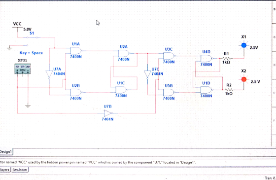
Master Slave D Flip Flop on Breadboard
Hello, I need major help on how to construct a MASTER-SLAVE D flip flop on a breadboard (Preferably a virtual one like tinkerCAD.com).

If you could upload a screenshot or picture of the final breadboard, that would help.
It can only use the following ICs: NOT (7404), 2-Input NAND (7400) or 2-Input NOR (7402).
It needs to be connected to a power supply, and LED's with resistors to test it out, thank you.
Label any of the wires if possible. I'd kindly appreciate this.
Please do not send the circuit diagram as I already have that. I do not know how to build it on the actual breadboard, thank you very much.
Homework Answers
Add Answer to:
Master Slave D Flip Flop on Breadboard
Hello, I need major help on how to construct...
Appreciate your help, This is a positive-edge-triggered master-slave D flip-flop. Dİ@ Clock Change this circuit to...
 Appreciate your help,
This is a positive-edge-triggered master-slave D flip-flop. Dİ@ Clock Change this circuit to a negative-edge-triggered master-slave D flip-flop. a. b. <Pre-Lab> <Pre-Lab> Draw the logic circuit. Draw the wiring diagram.
Appreciate your help,
This is a positive-edge-triggered master-slave D flip-flop. Dİ@ Clock Change this circuit to a negative-edge-triggered master-slave D flip-flop. a. b. <Pre-Lab> <Pre-Lab> Draw the logic circuit. Draw the wiring diagram.
Help please Below is a Master-Slave D Flip-Flop (positive edge triggered), sketch the waveform of Q_m...
 Help please
Below is a Master-Slave D Flip-Flop (positive edge triggered), sketch the waveform of Q_m and Q_s in the following timing diagram.
Help please
Below is a Master-Slave D Flip-Flop (positive edge triggered), sketch the waveform of Q_m and Q_s in the following timing diagram.
1. a) Complete the waveform templates for the Master –Slave D-flip-flop below with given D, CLK,...
 1.
a) Complete the waveform templates for the Master –Slave
D-flip-flop below with given D, CLK, CLEAR, and PRESET signals.
Neglect the propagation delays.
b) Does it have positive or negative edge triggering with
respect to CLK?
c) Are the asynchronous PRESET and CLEAR active-high or
active-low?
2. Enabling of data load in the D-flip-flop was implemented with
a 2-to-1 multiplexer as show below. The D-flip-flop has the
positive edge triggering and the active-low asynchronous clear.
a) Is the Enable...
1.
a) Complete the waveform templates for the Master –Slave
D-flip-flop below with given D, CLK, CLEAR, and PRESET signals.
Neglect the propagation delays.
b) Does it have positive or negative edge triggering with
respect to CLK?
c) Are the asynchronous PRESET and CLEAR active-high or
active-low?
2. Enabling of data load in the D-flip-flop was implemented with
a 2-to-1 multiplexer as show below. The D-flip-flop has the
positive edge triggering and the active-low asynchronous clear.
a) Is the Enable...
7. Construct the D-flip-flop with positive-edge triggering and asynchronous Clear (active-low). I...
 7. Construct the D-flip-flop with positive-edge triggering and asynchronous Clear (active-low). Implement the Master-Slave design with two gated D-latches from problem 6 as building blocks and inverters. a) b) Show the schematic. Complete the waveform template below (neglect the propagation delays). Qm and Q are the outputs of the Master and Slave D-latches, respectively. The initial state is unknown. CLK CLK bar CLEAR Qm
7. Construct the D-flip-flop with positive-edge triggering and asynchronous Clear (active-low). Implement the Master-Slave design with...
7. Construct the D-flip-flop with positive-edge triggering and asynchronous Clear (active-low). Implement the Master-Slave design with two gated D-latches from problem 6 as building blocks and inverters. a) b) Show the schematic. Complete the waveform template below (neglect the propagation delays). Qm and Q are the outputs of the Master and Slave D-latches, respectively. The initial state is unknown. CLK CLK bar CLEAR Qm
7. Construct the D-flip-flop with positive-edge triggering and asynchronous Clear (active-low). Implement the Master-Slave design with...
1. The D Flip-Flop ) Look for the datasheet of the 7474 D flip-flop and wire it on the breadboard...
 1. The D Flip-Flop ) Look for the datasheet of the 7474 D flip-flop and wire it on the breadboard making sure to supply 5V to both Preset and Clear. Utilize the function generator to provide a Clock signal of 1 Hz: i) Press AMPL and set value to 5 Vpp ii) Press FREQ and set value to 1 Hz ili) Press OFFSET and set value to 2.5 V This Clock signal will be the same for all circuits in...
3. Answer the following questions about a data flip-flop (D-Flip Flop): a) (4 ps) Write the VHDL required to define a rising-edge triggered (RET) D-Flip Flop with additional clock enable (CEN) an...
 3. Answer the following questions about a data flip-flop (D-Flip Flop): a) (4 ps) Write the VHDL required to define a rising-edge triggered (RET) D-Flip Flop with additional clock enable (CEN) and reset inputs. Your reset may be synchronous or asynchronous. Assume any input, output, or signal variables that you require have already been declared in VHDL (you do not have to write the declarations for these) b) [I pal ls your reset syachronous or asynchronous for the D-Flip Flop...
I NEED HELP WITH FLIP FLOPS Flip-flop type JK Design a JK flip flop using only...
I NEED HELP WITH FLIP FLOPS Flip-flop type JK Design a JK flip flop using only logic gates .Fill the truth table exercising all possible combinations of inputs for J and K Flip-flop type D Set the JK type flip flop from the previous step to work as a flip flop type D. Fill the truth table by exercising all combinations of possible entries D Flip-flop type T Set the circuit of the previous step to work as a flip...
Write the verilog code that implements a negitive edge D-Flip Flop with asynchronous active low preset...
Write the verilog code that implements a negitive edge D-Flip Flop with asynchronous active low preset and clear I have : module dff( preset, clear, clk, D, Q) input preset; input clear; input clk; input D; output Q; reg Q; always @ (negedge clk or negedge preset or negedge clear); if (preset); Q = 0; else (clear == 0); Q = D; endmodule I honestly just want to know if i'm doing this right or not, if im not correct,...
please solve this ASAP 4. (2.5pt) Latches A. (PDF) Implement a D flip-flop using 2 Dlatches...
 please solve this ASAP
4. (2.5pt) Latches A. (PDF) Implement a D flip-flop using 2 Dlatches without any SR nor SR latches, by drawing the circuit diagram by hand. (1pt) I B. Consider the standard latch implementation using logical gates as we've covered in class, discuss whether this alternative implementation is superior to the D-SR master-slave implementation approach in the box below. (0.5pt) Har.. meetings M Mathway | Algebra... assign mooodle CSCI 150: Introducti... Application Detail- WhatsApp C. (PDF) Extend...
please solve this ASAP
4. (2.5pt) Latches A. (PDF) Implement a D flip-flop using 2 Dlatches without any SR nor SR latches, by drawing the circuit diagram by hand. (1pt) I B. Consider the standard latch implementation using logical gates as we've covered in class, discuss whether this alternative implementation is superior to the D-SR master-slave implementation approach in the box below. (0.5pt) Har.. meetings M Mathway | Algebra... assign mooodle CSCI 150: Introducti... Application Detail- WhatsApp C. (PDF) Extend...
The lab can be made in orcad but all I need is how to and the...
 The lab can be made in orcad but all I need is how to
and the design. Please Read the problem carefully and answer as
much as you can. Thank you!!!
Part 2 T and D from JK 1. Using part 74107 (JK flip-flop), build a T and a D-flip. Do NOT put both designs on the same schematic page or in the same folder. 2. Create parts for each and run a simulation using the parts created. Part 3....
The lab can be made in orcad but all I need is how to
and the design. Please Read the problem carefully and answer as
much as you can. Thank you!!!
Part 2 T and D from JK 1. Using part 74107 (JK flip-flop), build a T and a D-flip. Do NOT put both designs on the same schematic page or in the same folder. 2. Create parts for each and run a simulation using the parts created. Part 3....
 Appreciate your help,
This is a positive-edge-triggered master-slave D flip-flop. Dİ@ Clock Change this circuit to a negative-edge-triggered master-slave D flip-flop. a. b. <Pre-Lab> <Pre-Lab> Draw the logic circuit. Draw the wiring diagram.
Appreciate your help,
This is a positive-edge-triggered master-slave D flip-flop. Dİ@ Clock Change this circuit to a negative-edge-triggered master-slave D flip-flop. a. b. <Pre-Lab> <Pre-Lab> Draw the logic circuit. Draw the wiring diagram.
 Help please
Below is a Master-Slave D Flip-Flop (positive edge triggered), sketch the waveform of Q_m and Q_s in the following timing diagram.
Help please
Below is a Master-Slave D Flip-Flop (positive edge triggered), sketch the waveform of Q_m and Q_s in the following timing diagram.
 1.
a) Complete the waveform templates for the Master –Slave
D-flip-flop below with given D, CLK, CLEAR, and PRESET signals.
Neglect the propagation delays.
b) Does it have positive or negative edge triggering with
respect to CLK?
c) Are the asynchronous PRESET and CLEAR active-high or
active-low?
2. Enabling of data load in the D-flip-flop was implemented with
a 2-to-1 multiplexer as show below. The D-flip-flop has the
positive edge triggering and the active-low asynchronous clear.
a) Is the Enable...
1.
a) Complete the waveform templates for the Master –Slave
D-flip-flop below with given D, CLK, CLEAR, and PRESET signals.
Neglect the propagation delays.
b) Does it have positive or negative edge triggering with
respect to CLK?
c) Are the asynchronous PRESET and CLEAR active-high or
active-low?
2. Enabling of data load in the D-flip-flop was implemented with
a 2-to-1 multiplexer as show below. The D-flip-flop has the
positive edge triggering and the active-low asynchronous clear.
a) Is the Enable...
 7. Construct the D-flip-flop with positive-edge triggering and asynchronous Clear (active-low). Implement the Master-Slave design with two gated D-latches from problem 6 as building blocks and inverters. a) b) Show the schematic. Complete the waveform template below (neglect the propagation delays). Qm and Q are the outputs of the Master and Slave D-latches, respectively. The initial state is unknown. CLK CLK bar CLEAR Qm
7. Construct the D-flip-flop with positive-edge triggering and asynchronous Clear (active-low). Implement the Master-Slave design with...
7. Construct the D-flip-flop with positive-edge triggering and asynchronous Clear (active-low). Implement the Master-Slave design with two gated D-latches from problem 6 as building blocks and inverters. a) b) Show the schematic. Complete the waveform template below (neglect the propagation delays). Qm and Q are the outputs of the Master and Slave D-latches, respectively. The initial state is unknown. CLK CLK bar CLEAR Qm
7. Construct the D-flip-flop with positive-edge triggering and asynchronous Clear (active-low). Implement the Master-Slave design with...
 1. The D Flip-Flop ) Look for the datasheet of the 7474 D flip-flop and wire it on the breadboard making sure to supply 5V to both Preset and Clear. Utilize the function generator to provide a Clock signal of 1 Hz: i) Press AMPL and set value to 5 Vpp ii) Press FREQ and set value to 1 Hz ili) Press OFFSET and set value to 2.5 V This Clock signal will be the same for all circuits in...
 3. Answer the following questions about a data flip-flop (D-Flip Flop): a) (4 ps) Write the VHDL required to define a rising-edge triggered (RET) D-Flip Flop with additional clock enable (CEN) and reset inputs. Your reset may be synchronous or asynchronous. Assume any input, output, or signal variables that you require have already been declared in VHDL (you do not have to write the declarations for these) b) [I pal ls your reset syachronous or asynchronous for the D-Flip Flop...
 please solve this ASAP
4. (2.5pt) Latches A. (PDF) Implement a D flip-flop using 2 Dlatches without any SR nor SR latches, by drawing the circuit diagram by hand. (1pt) I B. Consider the standard latch implementation using logical gates as we've covered in class, discuss whether this alternative implementation is superior to the D-SR master-slave implementation approach in the box below. (0.5pt) Har.. meetings M Mathway | Algebra... assign mooodle CSCI 150: Introducti... Application Detail- WhatsApp C. (PDF) Extend...
please solve this ASAP
4. (2.5pt) Latches A. (PDF) Implement a D flip-flop using 2 Dlatches without any SR nor SR latches, by drawing the circuit diagram by hand. (1pt) I B. Consider the standard latch implementation using logical gates as we've covered in class, discuss whether this alternative implementation is superior to the D-SR master-slave implementation approach in the box below. (0.5pt) Har.. meetings M Mathway | Algebra... assign mooodle CSCI 150: Introducti... Application Detail- WhatsApp C. (PDF) Extend...
 The lab can be made in orcad but all I need is how to
and the design. Please Read the problem carefully and answer as
much as you can. Thank you!!!
Part 2 T and D from JK 1. Using part 74107 (JK flip-flop), build a T and a D-flip. Do NOT put both designs on the same schematic page or in the same folder. 2. Create parts for each and run a simulation using the parts created. Part 3....
The lab can be made in orcad but all I need is how to
and the design. Please Read the problem carefully and answer as
much as you can. Thank you!!!
Part 2 T and D from JK 1. Using part 74107 (JK flip-flop), build a T and a D-flip. Do NOT put both designs on the same schematic page or in the same folder. 2. Create parts for each and run a simulation using the parts created. Part 3....
Most questions answered within 3 hours.
-
A .15kg rubber ball is bounced off a wall. Before hitting the
wall, the ball moves...
asked 28 minutes ago -
A manufacturing company preparing to build a new plant is
considering three potential locations for it....
asked 29 minutes ago -
B. If compound Y has approximately the same values of solubility
in toluene as compound X,...
asked 1 hour ago -
Oscar Inc. has inventory in Japan valued at 39,051,000 Yen one
year ago. One year ago...
asked 1 hour ago -
If Canada suffered from "fundamental disequilibrium," and its
government choose not to devalue its currency, a...
asked 1 hour ago -
4. How many input & output Key Value Pairs are passed into,
and emitted out of...
asked 1 hour ago -
Why would your heart not function well if constructed of
skeletal muscle? What is the particular...
asked 1 hour ago -
Please respond to this essay question in full essay form for
Chemistry 1102 Organic and Biochemistry:...
asked 1 hour ago -
Determine the head loss and velocity of flow in a water supply main
of 15.0 cm...
asked 1 hour ago -
A marketing executive who knowingly authorizes a shoddy
defective product to be brought to market is...
asked 1 hour ago -
Write a psudocode:
1. Define a function called authorize that takes in 2 strings,
uName, and...
asked 1 hour ago -
What Hall voltage (in mV) is produced by a 0.180 T field applied
across a 2.60...
asked 1 hour ago