
Homework Answers


Add Answer to:
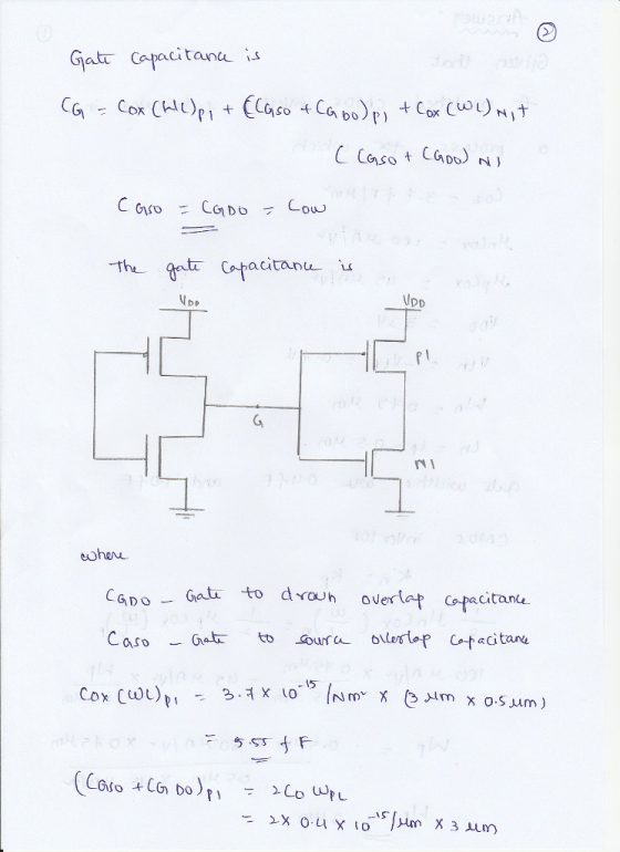
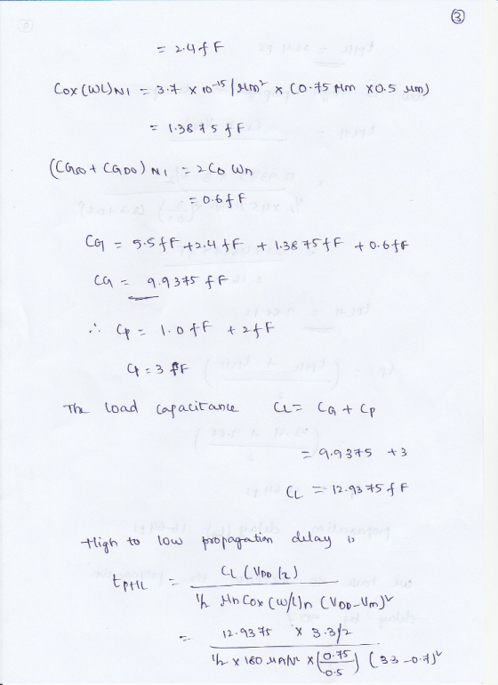
Problem 1 A matched CMOS inverter fabricated in a process for which Cor 3.7 fFjum2, μnCz-180...
For a CMOS inverter fabricated in a 0.18um process with the values given: Value Parameter (W/L)p ...
 For a CMOS inverter fabricated in a 0.18um process with the values given: Value Parameter (W/L)p (W/L)n 1.5 10fF 1.8V Vdd Use the equivalent resistance approach. What is the inverter propagation delay from low to high (tpLH)? Give your answer in pSec, number form to 2 decimal place, no units, no unit prefixes, no commas. Example: 10pS>Answer Given: 10.00
For a CMOS inverter fabricated in a 0.18um process with the values given: Value Parameter (W/L)p (W/L)n 1.5 10fF 1.8V Vdd...
For a CMOS inverter fabricated in a 0.18um process with the values given: Value Parameter (W/L)p (W/L)n 1.5 10fF 1.8V Vdd Use the equivalent resistance approach. What is the inverter propagation delay from low to high (tpLH)? Give your answer in pSec, number form to 2 decimal place, no units, no unit prefixes, no commas. Example: 10pS>Answer Given: 10.00
For a CMOS inverter fabricated in a 0.18um process with the values given: Value Parameter (W/L)p (W/L)n 1.5 10fF 1.8V Vdd...
14.31 Consider a CMOS inverter fabricated in a 65-nm CMOS process for which Vpp = 1V,...
 14.31 Consider a CMOS inverter fabricated in a 65-nm CMOS process for which Vpp = 1V, V = - = 0.35 V, and u C = 2.54 C = 470 HA/V'. In addition, ex and Q, have L = 65 nm and (WIL), = 1.5. (a) Find W that results in V = V 2. What is the silicon area utilized by the inverter in this case? (b) For the matched case in (a), find the values of Vow, VOL...
14.31 Consider a CMOS inverter fabricated in a 65-nm CMOS process for which VopV, V 0.35...
 14.31 Consider a CMOS inverter fabricated in a 65-nm CMOS process for which VopV, V 0.35 v and μη C ,-2.5μ, car-470 μΑ/V2. In addition, QN and QP have L 65 nm and (WIL), = 1.5 (a) Find W, that results in DD/2. What is the silicon area utilized by the inverter in this case? (b) For the matched case in (a), find the values of Vou, Vou» Vi, Vi, NM1, and NMH IH IL' (c) For the matched case...
a. Given a CMOS inverter has gate width Wn-20μm, channel length Lp-La- 2μm, process parameter Kp = 2.0x10⁻⁵A/V2, Kn = 5.0x10⁻⁵A/V2, find the value of (5 marks) the gate width Wp for Bp n b. Given...
 a. Given a CMOS inverter has gate width Wn-20μm, channel length Lp-La- 2μm, process parameter Kp = 2.0x10⁻⁵A/V2, Kn = 5.0x10⁻⁵A/V2, find the value of (5 marks) the gate width Wp for Bp n b. Given that the sheet resistance of the polysilicon is 4.0d the capacitance per unit area of the polysilicon is 0.1fF/um2. Calculate the time constant of a polysilicon polygon with structure shown in the figure, width equals to 3A and the (6 marks) corner resistance is...
A 6T SRAM cell is fabricated in a 0.18 ?m CMOS process for which VDD =...
 A 6T SRAM cell is fabricated in a 0.18 ?m CMOS process for which VDD = 1.8 V, V1-0.5 V, and HmC or 300 ??/V2. The inverters utilize (w/L)n I. Each of the bit lines has a 2 pF capacitance to a. Find the upper bound on WL for each of the access transistors so that Vo and Va do not change by b. Find the delay time ?t encountered in the read operation if the cell design utilizes minimum...
Table 1 Parameters for manual model of 0.13 micron CMOS process DSAT 0.416 0.39 0.297 254 0.14 NM...
 Table 1 Parameters for manual model of 0.13 micron CMOS process DSAT 0.416 0.39 0.297 254 0.14 NMOS PMOS -0.426 -0.29-0583 633 10261 Table 2 Capacitance parameters of NMOS and PMOS transistors in 0.13 micron CMOS process Cox Cov ma MOS 10.7 0.323 0.958 0.395 08 01 0288 0.8 P MOS-110.22ー10.298 11.02ー1042ー08 ー0.107ー0.1ーー0.8 (35 pt Q2 Inverter shown below is implemented in 0.13 um CMOS (8RF). The supply voltage is VDD-1.2 V. Both transistors have a channel length of 0.13...
 For a CMOS inverter fabricated in a 0.18um process with the values given: Value Parameter (W/L)p (W/L)n 1.5 10fF 1.8V Vdd Use the equivalent resistance approach. What is the inverter propagation delay from low to high (tpLH)? Give your answer in pSec, number form to 2 decimal place, no units, no unit prefixes, no commas. Example: 10pS>Answer Given: 10.00
For a CMOS inverter fabricated in a 0.18um process with the values given: Value Parameter (W/L)p (W/L)n 1.5 10fF 1.8V Vdd...
For a CMOS inverter fabricated in a 0.18um process with the values given: Value Parameter (W/L)p (W/L)n 1.5 10fF 1.8V Vdd Use the equivalent resistance approach. What is the inverter propagation delay from low to high (tpLH)? Give your answer in pSec, number form to 2 decimal place, no units, no unit prefixes, no commas. Example: 10pS>Answer Given: 10.00
For a CMOS inverter fabricated in a 0.18um process with the values given: Value Parameter (W/L)p (W/L)n 1.5 10fF 1.8V Vdd...
 14.31 Consider a CMOS inverter fabricated in a 65-nm CMOS process for which Vpp = 1V, V = - = 0.35 V, and u C = 2.54 C = 470 HA/V'. In addition, ex and Q, have L = 65 nm and (WIL), = 1.5. (a) Find W that results in V = V 2. What is the silicon area utilized by the inverter in this case? (b) For the matched case in (a), find the values of Vow, VOL...
 14.31 Consider a CMOS inverter fabricated in a 65-nm CMOS process for which VopV, V 0.35 v and μη C ,-2.5μ, car-470 μΑ/V2. In addition, QN and QP have L 65 nm and (WIL), = 1.5 (a) Find W, that results in DD/2. What is the silicon area utilized by the inverter in this case? (b) For the matched case in (a), find the values of Vou, Vou» Vi, Vi, NM1, and NMH IH IL' (c) For the matched case...
 a. Given a CMOS inverter has gate width Wn-20μm, channel length Lp-La- 2μm, process parameter Kp = 2.0x10⁻⁵A/V2, Kn = 5.0x10⁻⁵A/V2, find the value of (5 marks) the gate width Wp for Bp n b. Given that the sheet resistance of the polysilicon is 4.0d the capacitance per unit area of the polysilicon is 0.1fF/um2. Calculate the time constant of a polysilicon polygon with structure shown in the figure, width equals to 3A and the (6 marks) corner resistance is...
 A 6T SRAM cell is fabricated in a 0.18 ?m CMOS process for which VDD = 1.8 V, V1-0.5 V, and HmC or 300 ??/V2. The inverters utilize (w/L)n I. Each of the bit lines has a 2 pF capacitance to a. Find the upper bound on WL for each of the access transistors so that Vo and Va do not change by b. Find the delay time ?t encountered in the read operation if the cell design utilizes minimum...
 Table 1 Parameters for manual model of 0.13 micron CMOS process DSAT 0.416 0.39 0.297 254 0.14 NMOS PMOS -0.426 -0.29-0583 633 10261 Table 2 Capacitance parameters of NMOS and PMOS transistors in 0.13 micron CMOS process Cox Cov ma MOS 10.7 0.323 0.958 0.395 08 01 0288 0.8 P MOS-110.22ー10.298 11.02ー1042ー08 ー0.107ー0.1ーー0.8 (35 pt Q2 Inverter shown below is implemented in 0.13 um CMOS (8RF). The supply voltage is VDD-1.2 V. Both transistors have a channel length of 0.13...
Most questions answered within 3 hours.
-
A $1000 par value convertible bond has a conversion price of
$25. It is currently selling...
asked 1 minute from now -
import java.util.Arrays;
import java.util.Random;
import java.util.Scanner;
/**
* TODO Write a summary of the role of...
asked 1 minute ago -
Sodium hydroxide is a strong base and ammonium hydroxide is a
weak base. Which of the...
asked 7 minutes ago -
Glycerol, C3H8O3, is a substance used extensively in the
manufacture of cosmetics, foodstuffs, antifreeze, and plastics....
asked 10 minutes ago -
After moving through Chapter 1 of our textbook, what is a social
issue/area of concern that...
asked 10 minutes ago -
Please complete the implementation of the four functions IN
C.
//************************************************************************************/
//
// countNumberofOnes
//
//...
asked 30 minutes ago -
A memory test consists of 35 tasks. Each task is graded on a
scale of 1...
asked 11 minutes ago -
Construction Cost Analysis and Estimating:
A project requires 17,000 allowed hours. Location of the work is...
asked 19 minutes ago -
1: In 802.11b, Access Point (AP) delivers a nonce to the Station
(STA). This nonce is...
asked 20 minutes ago -
calculate change in entropy and change in enthalpy for freezing
1 mol of water at -10C...
asked 26 minutes ago -
In your opinion, did anyone "win" the Cold War? If no, why? If
yes, who won...
asked 30 minutes ago -
a) Determine the saturation dissolved oxygen concentration at
sea-level at 1 atm and 20° C in...
asked 28 minutes ago