

Homework Answers


Add Answer to:
2
photos
The depletion layer width for different junctions is given by the following equations: w...
3.13 Si pn junction Consider a long pn junction diode with an acceptor doping Naof 1018 cm-3 on t...
 3.13 Si pn junction Consider a long pn junction diode with an acceptor doping Naof 1018 cm-3 on the p-side and donor concentration of Nj on the n-side. The diode is forward biased and has a voltage of 0.6 V across it. The diode cross-sectional area is 1 mm2. The minority carrier recombination time, T, depends on the total dopant concentration, Ndopant (cm), through the following approximate empirical relation (5x 10⁻⁷)/(1 + 2 10-17N1°pan.) where T is in seconds. (a)...
Problem 4 (25 points) Consider a silicon pn junction at T-300 K, NA-ND- 1x101° cm3. The minority ...
 Problem 4 (25 points) Consider a silicon pn junction at T-300 K, NA-ND- 1x101° cm3. The minority carrier lifetimes are τ n-0.01 μs and τ p-0.01 us. The junction is forwardbiased with Va 0.6V. The minority carrier diffusion coefficients are Dn-20 cm s, Dp 10 cm Is. n.-1.5x 1010 cm-3 Depletion region n-type p-type a) (10 points) Calculate the excess electron concentration as a function of x in the p side (see the figure above). b) (5 points) Calculate the...
3.13 Si pn junction Consider a long pn junction diode with an acceptor doping Naof 1018...
 3.13 Si pn junction Consider a long pn junction diode with an acceptor doping Naof 1018 cm-3 on the p-side and donor concentration of Nj on the n-side. The diode is forward biased and has a voltage of 0.6 V across it. The diode cross-sectional area is 1 mm2. The minority carrier recombination time, T, depends on the total dopant concentration, Ndopant (cm), through the following approximate empirical relation (5x 10⁻⁷)/(1 + 2 10-17N1°pan.) where T is in seconds. (a)...
Problem 3 (25 points) Consider a silicon pn junction at T - 300 K, NA- 1016 cm3, ND-5x1016 cm-3. The minority carrier lifetimes are τα , τ,-1 us. The junction is forward biased with Va-0.5V The minor...
 Problem 3 (25 points) Consider a silicon pn junction at T - 300 K, NA- 1016 cm3, ND-5x1016 cm-3. The minority carrier lifetimes are τα , τ,-1 us. The junction is forward biased with Va-0.5V The minority carrier diffusion coefficients are D 25 cm/s, Da- 10 cm2/s n,1.5x1010 cm3 kT 0.0267 Depletion region p-type n-type a) (5 points) Calculate the excess electron concentration as a function of x in the p-side (see the figure above) b) (10 points) Calculate the...
Problem 4 (25 points) Consider a silicon pn junction at T-300 K, NA-ND- 1x101° cm3. The minority ...
 Can someone help solve this question step by step? Thanks!
Problem 4 (25 points) Consider a silicon pn junction at T-300 K, NA-ND- 1x101° cm3. The minority carrier lifetimes are τ n-0.01 μs and τ p-0.01 us. The junction is forwardbiased with Va 0.6V. The minority carrier diffusion coefficients are Dn-20 cm s, Dp 10 cm Is. n.-1.5x 1010 cm-3 Depletion region n-type p-type a) (10 points) Calculate the excess electron concentration as a function of x in the p...
Can someone help solve this question step by step? Thanks!
Problem 4 (25 points) Consider a silicon pn junction at T-300 K, NA-ND- 1x101° cm3. The minority carrier lifetimes are τ n-0.01 μs and τ p-0.01 us. The junction is forwardbiased with Va 0.6V. The minority carrier diffusion coefficients are Dn-20 cm s, Dp 10 cm Is. n.-1.5x 1010 cm-3 Depletion region n-type p-type a) (10 points) Calculate the excess electron concentration as a function of x in the p...
Consider a silicon pn junction at T = 300 K, NA-Np - 4x106cm. The minority carrier...
 Consider a silicon pn junction at T = 300 K, NA-Np - 4x106cm. The minority carrier lifetimes are tn = Tp=1 us. The junction is forward biased with V, -0.6V. The minority carrier diffusion coefficients are D = 20 cm²/s, D = 10 cm²/s. n;= 1.5x100cm, kt/e = 0.026V Depletion region n-type p-type a) (5 points) Do we have low-level injection? b) (10 points) Calculate the electron concentration at x = -(Xp + Ln) where L, is the electron diffusion...
this is a problem of semiconductor device and fundamentals. Problem 4: pn Junction Current Distributions Consider a...
 this is a problem of semiconductor device and
fundamentals.
Problem 4: pn Junction Current Distributions Consider a Si pn step junction diode maintained at room temperature, with p-side and n-side dopant concentrations NA 1016 cm3 and Np-2x1016 cm3, respectively. (You may assume that each side is uncompensated.) The minority carrier recombination lifetimes are τ,-10-6 s and τ,-10-7 s on the p-side and n-side, respectively a) Calculate the minority carrier densities at the edges of the depletion region when the applied...
this is a problem of semiconductor device and
fundamentals.
Problem 4: pn Junction Current Distributions Consider a Si pn step junction diode maintained at room temperature, with p-side and n-side dopant concentrations NA 1016 cm3 and Np-2x1016 cm3, respectively. (You may assume that each side is uncompensated.) The minority carrier recombination lifetimes are τ,-10-6 s and τ,-10-7 s on the p-side and n-side, respectively a) Calculate the minority carrier densities at the edges of the depletion region when the applied...
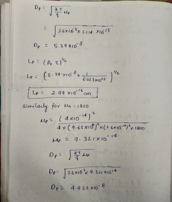
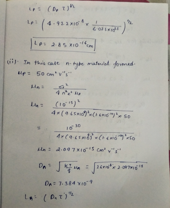
3. A silicon step junction has uniform impurity doping concentrations of N. 5 x 1015 cm-3 and Nd ...
 3. A silicon step junction has uniform impurity doping concentrations of N. 5 x 1015 cm-3 and Nd = 1 x 1015 cm-, and a cross-sectional area of A-|0-4 cm2. Let tao -0.4 s and tpo 0.1 us. Consider the geometry in Figure.Calculate (a) the ideal reverse saturation current due to holes, (b) the ideal reverse saturation current due to electrons, (c) the hole concentration at a, if V V and (d) the electron current at x = x" +...
A uniformly doped silicon pnp transistor with base width of 2um is biased in forward active mode (with BC junction reverse biased). The doping concentrations are NE-1018cm NB-5x1016cm3, and Nc-1015cm...
 A uniformly doped silicon pnp transistor with base width of 2um is biased in forward active mode (with BC junction reverse biased). The doping concentrations are NE-1018cm NB-5x1016cm3, and Nc-1015cm3. Assume DB-25 cm2/s, TB-10-s and LB 16um (a) Calculate the values of no, рво, and nco. (b) For VEB 0.65V, determine the respective minority carrier concentration at the edge of the depletion layer, pa(0) and ne(0) (c) Sketch the minority carrier concentration through the device and label each curve (d)...
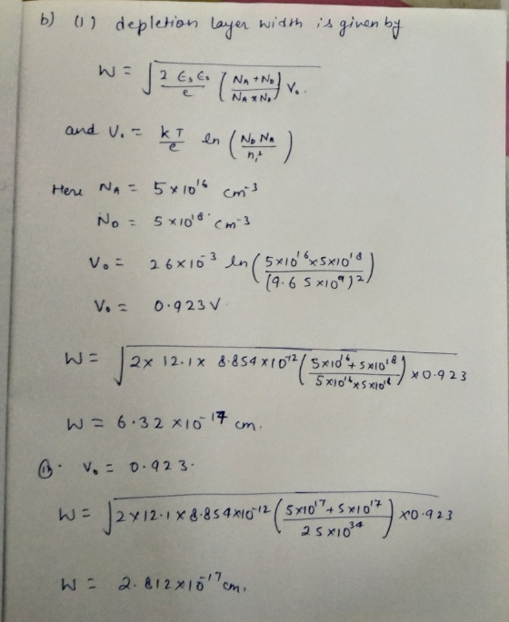
Design an ideal abrupt silicon PN-junction at 300 K such that the donor impurity concentration in...
 XXX is 467
Design an ideal abrupt silicon PN-junction at 300 K such that the donor impurity concentration in the n-side N, = 5x1015 cm3 and the acceptor impurity concentration in the p-side N, = XXX × 1015/cm3 Assume that the diode area A-2x10⁻³ cm2 and 100cm work Note that the values obtained in the calculations may not be realistic as the Matric # varies greatly. The assignment is only to test your understanding, and must be handwritten Determine the...
XXX is 467
Design an ideal abrupt silicon PN-junction at 300 K such that the donor impurity concentration in the n-side N, = 5x1015 cm3 and the acceptor impurity concentration in the p-side N, = XXX × 1015/cm3 Assume that the diode area A-2x10⁻³ cm2 and 100cm work Note that the values obtained in the calculations may not be realistic as the Matric # varies greatly. The assignment is only to test your understanding, and must be handwritten Determine the...
 3.13 Si pn junction Consider a long pn junction diode with an acceptor doping Naof 1018 cm-3 on the p-side and donor concentration of Nj on the n-side. The diode is forward biased and has a voltage of 0.6 V across it. The diode cross-sectional area is 1 mm2. The minority carrier recombination time, T, depends on the total dopant concentration, Ndopant (cm), through the following approximate empirical relation (5x 10⁻⁷)/(1 + 2 10-17N1°pan.) where T is in seconds. (a)...
 Problem 4 (25 points) Consider a silicon pn junction at T-300 K, NA-ND- 1x101° cm3. The minority carrier lifetimes are τ n-0.01 μs and τ p-0.01 us. The junction is forwardbiased with Va 0.6V. The minority carrier diffusion coefficients are Dn-20 cm s, Dp 10 cm Is. n.-1.5x 1010 cm-3 Depletion region n-type p-type a) (10 points) Calculate the excess electron concentration as a function of x in the p side (see the figure above). b) (5 points) Calculate the...
 3.13 Si pn junction Consider a long pn junction diode with an acceptor doping Naof 1018 cm-3 on the p-side and donor concentration of Nj on the n-side. The diode is forward biased and has a voltage of 0.6 V across it. The diode cross-sectional area is 1 mm2. The minority carrier recombination time, T, depends on the total dopant concentration, Ndopant (cm), through the following approximate empirical relation (5x 10⁻⁷)/(1 + 2 10-17N1°pan.) where T is in seconds. (a)...
 Problem 3 (25 points) Consider a silicon pn junction at T - 300 K, NA- 1016 cm3, ND-5x1016 cm-3. The minority carrier lifetimes are τα , τ,-1 us. The junction is forward biased with Va-0.5V The minority carrier diffusion coefficients are D 25 cm/s, Da- 10 cm2/s n,1.5x1010 cm3 kT 0.0267 Depletion region p-type n-type a) (5 points) Calculate the excess electron concentration as a function of x in the p-side (see the figure above) b) (10 points) Calculate the...
 Can someone help solve this question step by step? Thanks!
Problem 4 (25 points) Consider a silicon pn junction at T-300 K, NA-ND- 1x101° cm3. The minority carrier lifetimes are τ n-0.01 μs and τ p-0.01 us. The junction is forwardbiased with Va 0.6V. The minority carrier diffusion coefficients are Dn-20 cm s, Dp 10 cm Is. n.-1.5x 1010 cm-3 Depletion region n-type p-type a) (10 points) Calculate the excess electron concentration as a function of x in the p...
Can someone help solve this question step by step? Thanks!
Problem 4 (25 points) Consider a silicon pn junction at T-300 K, NA-ND- 1x101° cm3. The minority carrier lifetimes are τ n-0.01 μs and τ p-0.01 us. The junction is forwardbiased with Va 0.6V. The minority carrier diffusion coefficients are Dn-20 cm s, Dp 10 cm Is. n.-1.5x 1010 cm-3 Depletion region n-type p-type a) (10 points) Calculate the excess electron concentration as a function of x in the p...
 Consider a silicon pn junction at T = 300 K, NA-Np - 4x106cm. The minority carrier lifetimes are tn = Tp=1 us. The junction is forward biased with V, -0.6V. The minority carrier diffusion coefficients are D = 20 cm²/s, D = 10 cm²/s. n;= 1.5x100cm, kt/e = 0.026V Depletion region n-type p-type a) (5 points) Do we have low-level injection? b) (10 points) Calculate the electron concentration at x = -(Xp + Ln) where L, is the electron diffusion...
 this is a problem of semiconductor device and
fundamentals.
Problem 4: pn Junction Current Distributions Consider a Si pn step junction diode maintained at room temperature, with p-side and n-side dopant concentrations NA 1016 cm3 and Np-2x1016 cm3, respectively. (You may assume that each side is uncompensated.) The minority carrier recombination lifetimes are τ,-10-6 s and τ,-10-7 s on the p-side and n-side, respectively a) Calculate the minority carrier densities at the edges of the depletion region when the applied...
this is a problem of semiconductor device and
fundamentals.
Problem 4: pn Junction Current Distributions Consider a Si pn step junction diode maintained at room temperature, with p-side and n-side dopant concentrations NA 1016 cm3 and Np-2x1016 cm3, respectively. (You may assume that each side is uncompensated.) The minority carrier recombination lifetimes are τ,-10-6 s and τ,-10-7 s on the p-side and n-side, respectively a) Calculate the minority carrier densities at the edges of the depletion region when the applied...
 3. A silicon step junction has uniform impurity doping concentrations of N. 5 x 1015 cm-3 and Nd = 1 x 1015 cm-, and a cross-sectional area of A-|0-4 cm2. Let tao -0.4 s and tpo 0.1 us. Consider the geometry in Figure.Calculate (a) the ideal reverse saturation current due to holes, (b) the ideal reverse saturation current due to electrons, (c) the hole concentration at a, if V V and (d) the electron current at x = x" +...
 A uniformly doped silicon pnp transistor with base width of 2um is biased in forward active mode (with BC junction reverse biased). The doping concentrations are NE-1018cm NB-5x1016cm3, and Nc-1015cm3. Assume DB-25 cm2/s, TB-10-s and LB 16um (a) Calculate the values of no, рво, and nco. (b) For VEB 0.65V, determine the respective minority carrier concentration at the edge of the depletion layer, pa(0) and ne(0) (c) Sketch the minority carrier concentration through the device and label each curve (d)...
 XXX is 467
Design an ideal abrupt silicon PN-junction at 300 K such that the donor impurity concentration in the n-side N, = 5x1015 cm3 and the acceptor impurity concentration in the p-side N, = XXX × 1015/cm3 Assume that the diode area A-2x10⁻³ cm2 and 100cm work Note that the values obtained in the calculations may not be realistic as the Matric # varies greatly. The assignment is only to test your understanding, and must be handwritten Determine the...
XXX is 467
Design an ideal abrupt silicon PN-junction at 300 K such that the donor impurity concentration in the n-side N, = 5x1015 cm3 and the acceptor impurity concentration in the p-side N, = XXX × 1015/cm3 Assume that the diode area A-2x10⁻³ cm2 and 100cm work Note that the values obtained in the calculations may not be realistic as the Matric # varies greatly. The assignment is only to test your understanding, and must be handwritten Determine the...
Most questions answered within 3 hours.
-
Already famous by the time he arrived at Princeton University in
1933, Einstein had suggested a...
asked 12 minutes ago -
Suppose the average male brain weight (in grams) is estimated to
be 13201320 grams. A 1905...
asked 21 minutes ago -
For each molecular substance (a) H3PO2 and (b) C6H5NH2,
calculate its molecular mass and write a...
asked 14 minutes ago -
The inheritance of color blindness in humans is due to a
recessive gene located on the...
asked 17 minutes ago -
Aqueous sulfuric acid (H2SO4) reacts with solid sodium hydroxide
(NaOH) to produce aqueous sodium sulfate (Na2SO4)...
asked 18 minutes ago -
QUESTION 25:
Find the pure binary representation of the following decimal
value: You DO NOT need...
asked 21 minutes ago -
The English mathematician John Kerrich tossed a coin
10,000 times and obtained 5067 heads.
a. calculate...
asked 48 minutes ago -
13. Use the Student's t-distribution to find the t-value for
each of the given scenarios. Round...
asked 41 minutes ago -
Explain the nutrition assessment for the lower gastrointestinal
tract, including the components of client history, anthropometric...
asked 40 minutes ago -
1.Marc has tried to quit heroin seven times only to
relapse each and every time. Marc...
asked 48 minutes ago -
A process has an input as the flow q gal/min, and an
output temperature T Fahrenheit. Initially,...
asked 54 minutes ago -
A sample of 30 patients in a doctor's office showed that they
had to wait an...
asked 1 hour ago