
Homework Answers
Add Answer to:
x=4
Question 3: The parameters of both bjt are as follows: base emitter turn on voltage...
Perform a simple initial design of an ac coupled common-emitter amplifier with four resistor biasing and emitter by-pass...
 Perform a simple initial design of an ac coupled common-emitter
amplifier with
four resistor biasing and emitter by-pass capacitor, to have a
voltage gain of about
100, for the following conditions. Justify any approximations used.
(Assume Ic=1/300 A)
i)Transistor ac common-emitter gain, B, 100 ii) Supply voltage ofV0c-20V iii) Allow 10% Vcc across RE DC collector voltage of 10 V iv) v) DC current in the base bias resistors should be ten times greater than the DC base current. Assume...
Perform a simple initial design of an ac coupled common-emitter
amplifier with
four resistor biasing and emitter by-pass capacitor, to have a
voltage gain of about
100, for the following conditions. Justify any approximations used.
(Assume Ic=1/300 A)
i)Transistor ac common-emitter gain, B, 100 ii) Supply voltage ofV0c-20V iii) Allow 10% Vcc across RE DC collector voltage of 10 V iv) v) DC current in the base bias resistors should be ten times greater than the DC base current. Assume...
Shown below is a single stage common emitter amplifier with a unipolar dc power supply using an 2...
 Shown below is a single stage common emitter amplifier with a unipolar dc power supply using an 2N3904 NPN BJT as the active device. It is specified that V+ 40 V, C1 C2CE 100uF, Ro-7.5 k2, REi-5.1kS2, and Ri - 36k52. Design the circuit so that the dc collector current is 2 mA and the magnitude of the small-signal midband voltage gain is 32.3. For the design calculations assume that the base-to- emitter dc voltage drop is 0.65 V, the...
4. For the amplifier in the figure below use the parameters in the table: +Vcc Re VBE- 0.7V, Ri- ...
 4. For the amplifier in the figure below use the parameters in the table: +Vcc Re VBE- 0.7V, Ri- 1002, R1-160k2, R2-320k2 R3-200k2, R6-40 k2, Rc-60k2, Vcc- 12V, Ry Do a) Draw the DC equivalent circuit and calculate the Q-point. c) Draw the AC equivalent circuit with the small signal model for the transistor. d) Calculate the voltage gain, Av-Vo/vi. Assume ro infinite. e) Draw the circuit to find the amplifier input resistance (Rin). Calculate Rin f Draw the circuit...
1.0 kn. RE-390 Ω, r-15 Ω. and ßac-75. 5. For a common-emitter amplifier, Rc Assuming that Rg is completely bypassed at the operating frequency, the voltage gain is (a) 66.7 (d) 75 (b) 2.56 (c) 2....
 1.0 kn. RE-390 Ω, r-15 Ω. and ßac-75. 5. For a common-emitter amplifier, Rc Assuming that Rg is completely bypassed at the operating frequency, the voltage gain is (a) 66.7 (d) 75 (b) 2.56 (c) 2.47 6. In the circuit of Question 5, if the frequency is reduced to the point where Xctbypass) RE, the voltage gain (a) remains the same (b) is less (c) is greater 7. In a common-emitter amplifier with voltage-divider bias, Rimlbase) 68 k2, Ri 33...
HELP with finding 8 and 9 2. IC temperature sensor The emitter-base voltage VEB of a PNP bipolar junction transistor (BJT) with its base and collector shorted (figure 1(a)) can be expressed by VEB (k...
 HELP with finding 8 and 9
2. IC temperature sensor The emitter-base voltage VEB of a PNP bipolar junction transistor (BJT) with its base and collector shorted (figure 1(a)) can be expressed by VEB (kT/q) In(Ic/Is), in which Is is the saturation current of the emitter-base junction (a) (3 pts) Choose any statement below that correctly describe the effect of temperature on the property of the BIT under a constant 1c as shown in figure 1(a).18_.(one or more than one...
HELP with finding 8 and 9
2. IC temperature sensor The emitter-base voltage VEB of a PNP bipolar junction transistor (BJT) with its base and collector shorted (figure 1(a)) can be expressed by VEB (kT/q) In(Ic/Is), in which Is is the saturation current of the emitter-base junction (a) (3 pts) Choose any statement below that correctly describe the effect of temperature on the property of the BIT under a constant 1c as shown in figure 1(a).18_.(one or more than one...
4. Consider the following Common Base BJT circuit given in the figure below: i. Use the...
 4. Consider the following Common Base BJT circuit given in the figure below: i. Use the data sheets of CA3046 BJT array and design a common collector circuit given in the following Figure 2 with the stated specifications in Table 2 Clearly show your design procedure. (Hint: show your calculation steps for both DC and AC small signall analysis) ii. Important Note : Ifyou remove RE you should also remove ClI, that is, connecting ac voltage source directly to emitter)...
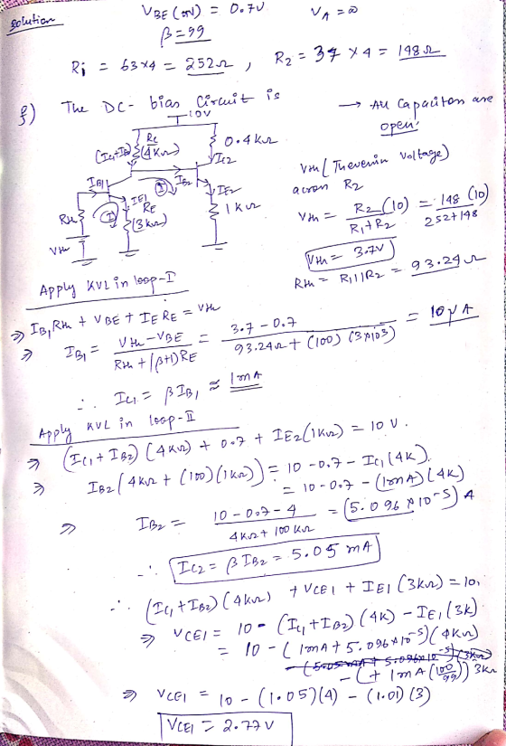
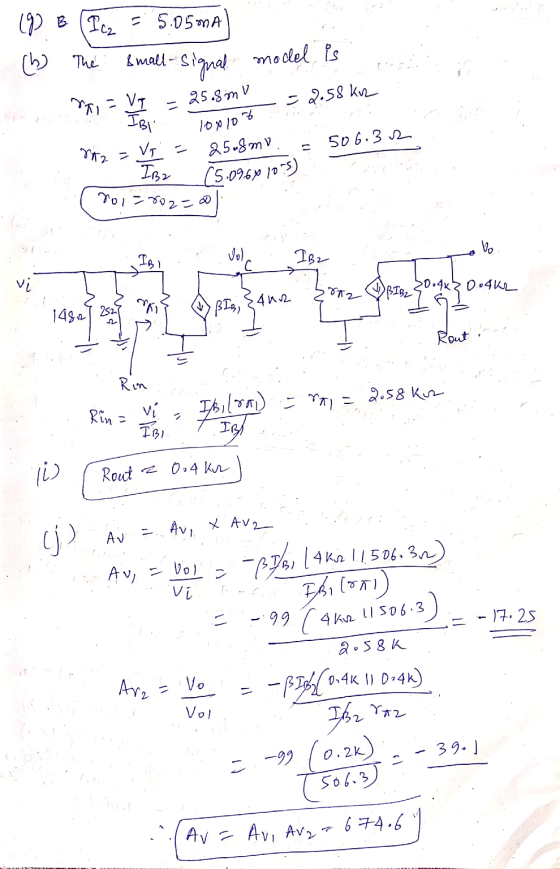
3. In Figure 3, the DC operating point for BJT Q, is Ici = 170 uA...
 3. In Figure 3, the DC operating point for BJT Q, is Ici = 170 uA and VCE = 4 V, and the DC operating point for BJT 02 is Ic2 = 240 A and VCE2 = 3 V. Both Q1 and Q2 have B = 100, VA-75 V at the room temperature. Assume that all the capacitors have infinite values, and all the resistors have the values as indicated in Figure 3. (a) (b) Determine the voltage gain 4....
A common-emitter BJT amplificr is shown in Fig.8.1. Note the DC biasing values and the BJTsmall-s...
 A common-emitter BJT amplificr is shown in Fig.8.1. Note the DC biasing values and the BJTsmall-signalmodel parameters from the class-signment #9 on DC Bia ing. Neglect the value of Rs in your calculations, k1 Rs-a k2: 1· Cal ulatethesmall-agalpannetas ofthe amplifi randcompletethecalculated valuesinTable8-1 Smalls-signal voltage gai, AVk Small-signal input resistance,k, Small-signaloutput resistance, Ro VW RC 2k C2 RB 570k Rs C1 1 10uP 0.1m 1 Vs CE RE 2k SINE(0 1mV 1kHz 0 0 00) tran 0 2ms 0 1us...
1-Clear handwriting 2-Correct answer 3-Organized 4-answer all the questions Please Problem 2 On the circuit on...
 1-Clear handwriting
2-Correct answer
3-Organized
4-answer all the questions
Please
Problem 2 On the circuit on Figure P2, transi stor Q1 has a threshold voltage of Vt = 2 V and a transconductance parameter of k = 100 mA/V2. Note that Vcc = -Vee = 4.5 V. Moreover, capacitors C1, C2, and C3 can be assumed to be very large VDD 4.5.0 R3 25kQ R1 300kn C2 Vout C1 Rsig Q1 1k0 R2 200kn Vsig (R4 2kQ C3 -4.5V VSS...
1-Clear handwriting
2-Correct answer
3-Organized
4-answer all the questions
Please
Problem 2 On the circuit on Figure P2, transi stor Q1 has a threshold voltage of Vt = 2 V and a transconductance parameter of k = 100 mA/V2. Note that Vcc = -Vee = 4.5 V. Moreover, capacitors C1, C2, and C3 can be assumed to be very large VDD 4.5.0 R3 25kQ R1 300kn C2 Vout C1 Rsig Q1 1k0 R2 200kn Vsig (R4 2kQ C3 -4.5V VSS...
It Kind of goes without saying but if you have no knowledge than dont comment or try and answer this question you dope Questions 1-3 below are about the amplifier circuit of Figure 1. Here Vcc is a...
 It
Kind of goes without saying but if you have no knowledge than dont
comment or try and answer this question you dope
Questions 1-3 below are about the amplifier circuit of Figure 1. Here Vcc is a fixed voltage The base voltage vB(t) is time-varying, and is of the form vB(t) V(t) where VB is a DC offset, and vb(t) is a time-varying purely AC signal. Suppose the amplitude of vb is A. Assume that the capacitor C is...
It
Kind of goes without saying but if you have no knowledge than dont
comment or try and answer this question you dope
Questions 1-3 below are about the amplifier circuit of Figure 1. Here Vcc is a fixed voltage The base voltage vB(t) is time-varying, and is of the form vB(t) V(t) where VB is a DC offset, and vb(t) is a time-varying purely AC signal. Suppose the amplitude of vb is A. Assume that the capacitor C is...
 Perform a simple initial design of an ac coupled common-emitter
amplifier with
four resistor biasing and emitter by-pass capacitor, to have a
voltage gain of about
100, for the following conditions. Justify any approximations used.
(Assume Ic=1/300 A)
i)Transistor ac common-emitter gain, B, 100 ii) Supply voltage ofV0c-20V iii) Allow 10% Vcc across RE DC collector voltage of 10 V iv) v) DC current in the base bias resistors should be ten times greater than the DC base current. Assume...
Perform a simple initial design of an ac coupled common-emitter
amplifier with
four resistor biasing and emitter by-pass capacitor, to have a
voltage gain of about
100, for the following conditions. Justify any approximations used.
(Assume Ic=1/300 A)
i)Transistor ac common-emitter gain, B, 100 ii) Supply voltage ofV0c-20V iii) Allow 10% Vcc across RE DC collector voltage of 10 V iv) v) DC current in the base bias resistors should be ten times greater than the DC base current. Assume...
 Shown below is a single stage common emitter amplifier with a unipolar dc power supply using an 2N3904 NPN BJT as the active device. It is specified that V+ 40 V, C1 C2CE 100uF, Ro-7.5 k2, REi-5.1kS2, and Ri - 36k52. Design the circuit so that the dc collector current is 2 mA and the magnitude of the small-signal midband voltage gain is 32.3. For the design calculations assume that the base-to- emitter dc voltage drop is 0.65 V, the...
 4. For the amplifier in the figure below use the parameters in the table: +Vcc Re VBE- 0.7V, Ri- 1002, R1-160k2, R2-320k2 R3-200k2, R6-40 k2, Rc-60k2, Vcc- 12V, Ry Do a) Draw the DC equivalent circuit and calculate the Q-point. c) Draw the AC equivalent circuit with the small signal model for the transistor. d) Calculate the voltage gain, Av-Vo/vi. Assume ro infinite. e) Draw the circuit to find the amplifier input resistance (Rin). Calculate Rin f Draw the circuit...
 1.0 kn. RE-390 Ω, r-15 Ω. and ßac-75. 5. For a common-emitter amplifier, Rc Assuming that Rg is completely bypassed at the operating frequency, the voltage gain is (a) 66.7 (d) 75 (b) 2.56 (c) 2.47 6. In the circuit of Question 5, if the frequency is reduced to the point where Xctbypass) RE, the voltage gain (a) remains the same (b) is less (c) is greater 7. In a common-emitter amplifier with voltage-divider bias, Rimlbase) 68 k2, Ri 33...
 HELP with finding 8 and 9
2. IC temperature sensor The emitter-base voltage VEB of a PNP bipolar junction transistor (BJT) with its base and collector shorted (figure 1(a)) can be expressed by VEB (kT/q) In(Ic/Is), in which Is is the saturation current of the emitter-base junction (a) (3 pts) Choose any statement below that correctly describe the effect of temperature on the property of the BIT under a constant 1c as shown in figure 1(a).18_.(one or more than one...
HELP with finding 8 and 9
2. IC temperature sensor The emitter-base voltage VEB of a PNP bipolar junction transistor (BJT) with its base and collector shorted (figure 1(a)) can be expressed by VEB (kT/q) In(Ic/Is), in which Is is the saturation current of the emitter-base junction (a) (3 pts) Choose any statement below that correctly describe the effect of temperature on the property of the BIT under a constant 1c as shown in figure 1(a).18_.(one or more than one...
 4. Consider the following Common Base BJT circuit given in the figure below: i. Use the data sheets of CA3046 BJT array and design a common collector circuit given in the following Figure 2 with the stated specifications in Table 2 Clearly show your design procedure. (Hint: show your calculation steps for both DC and AC small signall analysis) ii. Important Note : Ifyou remove RE you should also remove ClI, that is, connecting ac voltage source directly to emitter)...
 3. In Figure 3, the DC operating point for BJT Q, is Ici = 170 uA and VCE = 4 V, and the DC operating point for BJT 02 is Ic2 = 240 A and VCE2 = 3 V. Both Q1 and Q2 have B = 100, VA-75 V at the room temperature. Assume that all the capacitors have infinite values, and all the resistors have the values as indicated in Figure 3. (a) (b) Determine the voltage gain 4....
 A common-emitter BJT amplificr is shown in Fig.8.1. Note the DC biasing values and the BJTsmall-signalmodel parameters from the class-signment #9 on DC Bia ing. Neglect the value of Rs in your calculations, k1 Rs-a k2: 1· Cal ulatethesmall-agalpannetas ofthe amplifi randcompletethecalculated valuesinTable8-1 Smalls-signal voltage gai, AVk Small-signal input resistance,k, Small-signaloutput resistance, Ro VW RC 2k C2 RB 570k Rs C1 1 10uP 0.1m 1 Vs CE RE 2k SINE(0 1mV 1kHz 0 0 00) tran 0 2ms 0 1us...
 1-Clear handwriting
2-Correct answer
3-Organized
4-answer all the questions
Please
Problem 2 On the circuit on Figure P2, transi stor Q1 has a threshold voltage of Vt = 2 V and a transconductance parameter of k = 100 mA/V2. Note that Vcc = -Vee = 4.5 V. Moreover, capacitors C1, C2, and C3 can be assumed to be very large VDD 4.5.0 R3 25kQ R1 300kn C2 Vout C1 Rsig Q1 1k0 R2 200kn Vsig (R4 2kQ C3 -4.5V VSS...
1-Clear handwriting
2-Correct answer
3-Organized
4-answer all the questions
Please
Problem 2 On the circuit on Figure P2, transi stor Q1 has a threshold voltage of Vt = 2 V and a transconductance parameter of k = 100 mA/V2. Note that Vcc = -Vee = 4.5 V. Moreover, capacitors C1, C2, and C3 can be assumed to be very large VDD 4.5.0 R3 25kQ R1 300kn C2 Vout C1 Rsig Q1 1k0 R2 200kn Vsig (R4 2kQ C3 -4.5V VSS...
 It
Kind of goes without saying but if you have no knowledge than dont
comment or try and answer this question you dope
Questions 1-3 below are about the amplifier circuit of Figure 1. Here Vcc is a fixed voltage The base voltage vB(t) is time-varying, and is of the form vB(t) V(t) where VB is a DC offset, and vb(t) is a time-varying purely AC signal. Suppose the amplitude of vb is A. Assume that the capacitor C is...
It
Kind of goes without saying but if you have no knowledge than dont
comment or try and answer this question you dope
Questions 1-3 below are about the amplifier circuit of Figure 1. Here Vcc is a fixed voltage The base voltage vB(t) is time-varying, and is of the form vB(t) V(t) where VB is a DC offset, and vb(t) is a time-varying purely AC signal. Suppose the amplitude of vb is A. Assume that the capacitor C is...
Most questions answered within 3 hours.
-
A business executive has the option to invest money in two
plans: Plan A guarantees that...
asked 40 minutes ago -
Hello, can someone please help me answer this question?
How much heat is absorbed by a...
asked 38 minutes ago -
. A marketing researcher conducted a survey of 25 shoppers
randomly selected at the local mall...
asked 54 minutes ago -
Create an comprehensive response to the
following:
Antimicrobial agents work on a multitude of microbes (bacteria,...
asked 56 minutes ago -
6.13 LAB: Step counter. Section 6.3.
A pedometer treats walking 2,000 steps as walking 1 mile....
asked 51 minutes ago -
(14.2) A block of mass m = 10 kg riding on a frictionless
horizontal plane is...
asked 55 minutes ago -
Use any search engine to search for articles about Starbucks
partnership with Tata Companies in India...
asked 53 minutes ago -
Let’s say that for some reason Bank Excess Reserves suddenly
increase sharply. What effect would this...
asked 1 hour ago -
Given:
Curent Assets: $600,000
Total Assets: $2,600,000
Current Liabilities: $500,000
Total Liabilities: $1,700,000
What is the...
asked 1 hour ago -
1. What is a “Bankster”? What is insider trading? Why is it
illegal?
2. What is...
asked 1 hour ago -
A transverse wave on a cord is given by
D(x,t)=0.18sin(2.7x−61.0t), where Dand x are in m...
asked 1 hour ago -
ASSIGNMENT
ANSWER ANY TWO OF THE FOLLOWING IN 2-3 PARAGRAPHS OF EACH
QUESTION.
1: Where is...
asked 1 hour ago