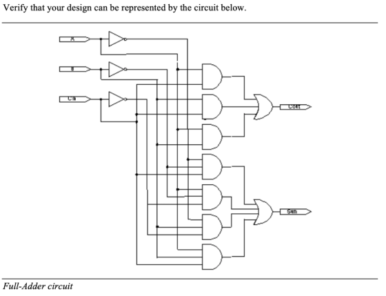

Many of the logic gates you require may not exist in standard TTL/CMOS 74 series family of logic. For example in future designs you may require a 50 input OR gate. The 74 series does not have a 50 input OR gate. For your 1 bit adder you will have the following devices: 1 quad 2 IP NAND, 1 TRIPLE 3 IP NAND, 7400 7410 7404 7420 1 HEX INVERTER, 1 DUAL 4 IP NAND, Use Boolean algebra to determine how you will use these gates and draw the circuit below
Homework Answers


Add Answer to:
Verify that your design can be represented by the circuit below. 120 Full-Adder circuit Many of...
5) Following is a NAND only 1-bit full adder circuit diagram. Using this 1-bit full adder...
 5) Following is a NAND only 1-bit full adder circuit diagram. Using this 1-bit full adder a 128-bit combined addition / subtraction circuit (ripple carry implementation) with overflow detection has been implemented using only 2-input NAND logic gate. What is the minimum number of NAND gates required for this circuit? [4pts) CI- Toyota
2. Design a 1 bit full adder (inputs:A,B,CARRY_IN - outputs:SUM,CARRY_OUT) using: (a) basic CMOS gates: inverter,...
 2. Design a 1 bit full adder (inputs:A,B,CARRY_IN - outputs:SUM,CARRY_OUT) using: (a) basic CMOS gates: inverter, NOR and NAND gates (b) complex CMOS logic gates and inverters (c) compare the difference in transistor counts (d) assuming all transistors are the same size and kn'= kp', which version of the function do you expect to be faster? Why?
AT&T 8:14 AM 100% < Back ECE204.Lab09-DataSheet.docx Гђ ECE 204 Lab 09 Basic Logic Gates Name: Na...
 AT&T 8:14 AM 100% < Back ECE204.Lab09-DataSheet.docx Гђ ECE 204 Lab 09 Basic Logic Gates Name: Name: Purpose: Replace this with a statement of purpose. Procedure A Digital input output test setup The digital circuits built throughout the rest of this lab will have the basic input and output setup as shown in Figure 1 Figure: Digital circuit input and output test setup The components for this setup include single throw dual pole switches and an LED. Figure 2 shows...
NAND can do it all! a functioning integrated circuit. Now is your time to create a...
 NAND can do it all! a functioning integrated circuit. Now is your time to create a circuit using only NAND gates. 1. Using the function: F (A B) (C D) Implement this function using AND and OR gates. Use the logic converterto assess your circuit. Imagine that you have no access to AND or OR gates. Create a circuit that implements the same function using only NANDgates. Use the Logic Converterto assess your NAND circuit. Compare to the previous AND/OR...
please anwer all the part of this lab and please use multisim. Lab 4: Basic Logic...
 please anwer all the part of this lab and please use
multisim.
Lab 4: Basic Logic Gates and Multisim Tools Objectives: • Learn to use the Logic Converter in Multisim to generate truth tables, design circuits and simplify logic expressions. • Build logic circuits using basic TTL gates. Software and Materials: • Multisim One 7400 (quad 2-input NAND gate) IC chip Procedure: 1. Write a logic expression for the circuit below. Have your instructor check the expression. А B с...
please anwer all the part of this lab and please use
multisim.
Lab 4: Basic Logic Gates and Multisim Tools Objectives: • Learn to use the Logic Converter in Multisim to generate truth tables, design circuits and simplify logic expressions. • Build logic circuits using basic TTL gates. Software and Materials: • Multisim One 7400 (quad 2-input NAND gate) IC chip Procedure: 1. Write a logic expression for the circuit below. Have your instructor check the expression. А B с...
Provide a breadboard schematic and expected output timing diagram showing how your circuit should behave Using...
Provide a breadboard schematic and expected output timing diagram showing how your circuit should behave Using any combination of the following components: 2 74HC00 quad 2-input NAND gate IC 1 74HC04 hex inverter IC 2 74HC08 quad 2-input AND gate IC 2 74HC32 quad 2-input OR gate IC 3 74HC74 dual D positive edge triggered flip-flop IC 1 74HC86 quad 2-input XOR gate IC 1 74HC157 quad 2-input multiplexer IC 1 CD74HCT390 dual decade counter IC 1 71256 32Kx8 SRAM...
CMOS Design Styles Quiz Problem 1: a) What is the typical "topology" for pMOS and nMOS...
CMOS Design Styles Quiz Problem 1: a) What is the typical "topology" for pMOS and nMOS in digital circuitry? -pMOS Vdd to Vout, nMOS Vout to Gnd -nMOS Vdd to Vout, pMOS Vout to Gnd -pMOS Vdd to Gnd, nMOS Vin to Vout -Only use xMOS -Both transistors Vin to Vout b) How do you implement nMOS in AND functions? -series connected, with increased widths -Parallel connected, with standard widths -Series connected with half the widths -Parallel connected, alternating large...
4. Design a 4-bit Adder / Subtractor. Follow the steps given below. (a) Write the VHDL...
 4. Design a 4-bit Adder / Subtractor. Follow the steps given below. (a) Write the VHDL code for a 1-bit Full Adder. The VHDL code must include an entity and an architecture. (b) Draw the circuit diagram for a 4-bit Adder / Subtractor. The circuit diagram may include the following logic elements: 1-bit Full Adders (shown as a block with inputs and outputs) Any 2-input logic gates Multiplexers Do not draw the logic circuit for the 1-bit Full Adder.
need help please thanks! Draw a gate-level schematic for the fall-adder module. XOR gates can be...
 need help please thanks!
Draw a gate-level schematic for the fall-adder module. XOR gates can be used to usplement Sotput; two levels ofNAND ples are handy for tn lema îngC, as a sum of products Create a MOSFET cirout for each of the logic gates you used in step 1 Your lab assigment this week is to design and test a CMOS circuit that performs addition Some suggestions on how to proceed Let's start with a simple ripple-cany adder based...
need help please thanks!
Draw a gate-level schematic for the fall-adder module. XOR gates can be used to usplement Sotput; two levels ofNAND ples are handy for tn lema îngC, as a sum of products Create a MOSFET cirout for each of the logic gates you used in step 1 Your lab assigment this week is to design and test a CMOS circuit that performs addition Some suggestions on how to proceed Let's start with a simple ripple-cany adder based...
please help question 2 2. Design a half-adder with the constraint that you can only use...
 please help question 2
2. Design a half-adder with the constraint that you can only use NAND and NOR gates. The circuit inputs are two bits I and y and the outputs are the sum bit s and carry bit c. Draw a circuit diagram and label each input and output. 3. The digital circuit below contains a latch and two flip-flops. Use the wave forms provided to find Qa. Qb, and Qe. Assume that all three states have initial...
please help question 2
2. Design a half-adder with the constraint that you can only use NAND and NOR gates. The circuit inputs are two bits I and y and the outputs are the sum bit s and carry bit c. Draw a circuit diagram and label each input and output. 3. The digital circuit below contains a latch and two flip-flops. Use the wave forms provided to find Qa. Qb, and Qe. Assume that all three states have initial...
 5) Following is a NAND only 1-bit full adder circuit diagram. Using this 1-bit full adder a 128-bit combined addition / subtraction circuit (ripple carry implementation) with overflow detection has been implemented using only 2-input NAND logic gate. What is the minimum number of NAND gates required for this circuit? [4pts) CI- Toyota
 2. Design a 1 bit full adder (inputs:A,B,CARRY_IN - outputs:SUM,CARRY_OUT) using: (a) basic CMOS gates: inverter, NOR and NAND gates (b) complex CMOS logic gates and inverters (c) compare the difference in transistor counts (d) assuming all transistors are the same size and kn'= kp', which version of the function do you expect to be faster? Why?
 AT&T 8:14 AM 100% < Back ECE204.Lab09-DataSheet.docx Гђ ECE 204 Lab 09 Basic Logic Gates Name: Name: Purpose: Replace this with a statement of purpose. Procedure A Digital input output test setup The digital circuits built throughout the rest of this lab will have the basic input and output setup as shown in Figure 1 Figure: Digital circuit input and output test setup The components for this setup include single throw dual pole switches and an LED. Figure 2 shows...
 NAND can do it all! a functioning integrated circuit. Now is your time to create a circuit using only NAND gates. 1. Using the function: F (A B) (C D) Implement this function using AND and OR gates. Use the logic converterto assess your circuit. Imagine that you have no access to AND or OR gates. Create a circuit that implements the same function using only NANDgates. Use the Logic Converterto assess your NAND circuit. Compare to the previous AND/OR...
 please anwer all the part of this lab and please use
multisim.
Lab 4: Basic Logic Gates and Multisim Tools Objectives: • Learn to use the Logic Converter in Multisim to generate truth tables, design circuits and simplify logic expressions. • Build logic circuits using basic TTL gates. Software and Materials: • Multisim One 7400 (quad 2-input NAND gate) IC chip Procedure: 1. Write a logic expression for the circuit below. Have your instructor check the expression. А B с...
please anwer all the part of this lab and please use
multisim.
Lab 4: Basic Logic Gates and Multisim Tools Objectives: • Learn to use the Logic Converter in Multisim to generate truth tables, design circuits and simplify logic expressions. • Build logic circuits using basic TTL gates. Software and Materials: • Multisim One 7400 (quad 2-input NAND gate) IC chip Procedure: 1. Write a logic expression for the circuit below. Have your instructor check the expression. А B с...
 4. Design a 4-bit Adder / Subtractor. Follow the steps given below. (a) Write the VHDL code for a 1-bit Full Adder. The VHDL code must include an entity and an architecture. (b) Draw the circuit diagram for a 4-bit Adder / Subtractor. The circuit diagram may include the following logic elements: 1-bit Full Adders (shown as a block with inputs and outputs) Any 2-input logic gates Multiplexers Do not draw the logic circuit for the 1-bit Full Adder.
 need help please thanks!
Draw a gate-level schematic for the fall-adder module. XOR gates can be used to usplement Sotput; two levels ofNAND ples are handy for tn lema îngC, as a sum of products Create a MOSFET cirout for each of the logic gates you used in step 1 Your lab assigment this week is to design and test a CMOS circuit that performs addition Some suggestions on how to proceed Let's start with a simple ripple-cany adder based...
need help please thanks!
Draw a gate-level schematic for the fall-adder module. XOR gates can be used to usplement Sotput; two levels ofNAND ples are handy for tn lema îngC, as a sum of products Create a MOSFET cirout for each of the logic gates you used in step 1 Your lab assigment this week is to design and test a CMOS circuit that performs addition Some suggestions on how to proceed Let's start with a simple ripple-cany adder based...
 please help question 2
2. Design a half-adder with the constraint that you can only use NAND and NOR gates. The circuit inputs are two bits I and y and the outputs are the sum bit s and carry bit c. Draw a circuit diagram and label each input and output. 3. The digital circuit below contains a latch and two flip-flops. Use the wave forms provided to find Qa. Qb, and Qe. Assume that all three states have initial...
please help question 2
2. Design a half-adder with the constraint that you can only use NAND and NOR gates. The circuit inputs are two bits I and y and the outputs are the sum bit s and carry bit c. Draw a circuit diagram and label each input and output. 3. The digital circuit below contains a latch and two flip-flops. Use the wave forms provided to find Qa. Qb, and Qe. Assume that all three states have initial...
Most questions answered within 3 hours.
-
The pH of a sample of water from a river is 5.0. A
sample of effluent from...
asked 5 minutes ago -
At the beginning of the period, the Fabricating Department
budgeted direct labor of $136,500 and equipment...
asked 32 minutes ago -
Please answer all
____ 28. Rent control is usually
justified on the grounds that it protects...
asked 32 minutes ago -
PARTS A-D HAVE BEEN ANSWERED. WAS TOLD TO REPOST. ONLY ANSWER
PARTS E and F.
A...
asked 50 minutes ago -
2) You are given the task of finding a representation for a
circle in a drawing...
asked 1 hour ago -
STUDY QUESTION: Does use of diet drug fen-phen
(fenfluramine-phentermine) cause valvular heart disease?
HINT: Valvular heart...
asked 1 hour ago -
1. An object weighing 40 N rests on a surface. The coefficient
of friction is 0.35....
asked 3 hours ago -
Investor company owns 35% of investee company voting stock and
accounts for the investment under the...
asked 4 hours ago -
The number of major faults on a randomly chosen 1 km stretch of
highway has a...
asked 4 hours ago -
Consider the competitive environment of Starbuck's, Progressive
Insurance, a manufacturing firm with low turnover, or a...
asked 5 hours ago -
3. Gains from trade
Consider two neighbouring island countries called Euphoria and
Contente. They each have...
asked 7 hours ago -
A business executive has the option to invest money in two
plans: Plan A guarantees that...
asked 9 hours ago