write step by step clear solution, NO INCOMPLETE OR SPAM answers accepted as will be directly complained and reported. ANSWER ALL QUESTIONS OR DONT ANSWER AT ALL! Please only answer if you are familiar and know how to do it, if you dont know, dont answer.
Homework Answers

Add Answer to:
write step by step clear solution, NO INCOMPLETE OR SPAM answers accepted as will be directly complained and reported. ANSWER ALL QUESTIONS OR DONT ANSWER AT ALL! Please only answer if you are familia...
Please Solve ALL parts. For the amplifier below, the MOSFET has the following parameters: VIV, k...
 Please Solve ALL parts.
For the amplifier below, the MOSFET has the following parameters: VIV, k 1) Show (prove) that the transistor operates in the saturation mode 2) Determine the operating point by finding In and VDs 3) Assume infinite values for the coupling capacitors and draw a small signal model for this amplifier ) Find gm and ro 5) Find the voltage gain (vo/vi) Find Ri 7) Find the current gain (ioli) VDD +12V RD- 10k2 Vo Vi lmA...
Please Solve ALL parts.
For the amplifier below, the MOSFET has the following parameters: VIV, k 1) Show (prove) that the transistor operates in the saturation mode 2) Determine the operating point by finding In and VDs 3) Assume infinite values for the coupling capacitors and draw a small signal model for this amplifier ) Find gm and ro 5) Find the voltage gain (vo/vi) Find Ri 7) Find the current gain (ioli) VDD +12V RD- 10k2 Vo Vi lmA...
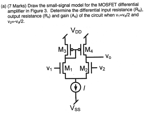
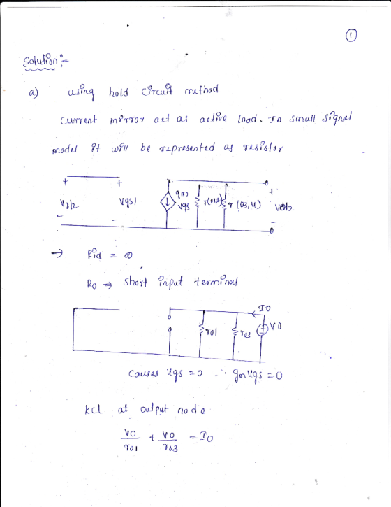
4) Consider the MOSFET differential amplifier shown below, with Io-2 mA, and RL- 10 kS2, Rss-100 ...
 4) Consider the MOSFET differential amplifier shown below, with Io-2 mA, and RL- 10 kS2, Rss-100 k2, VDD- +8V and Vss--8V. The NMOS transistors in the circuit are nominally identical, with kn 2 mA/V2, VTn 1.0 V and ro 100 k2. The PMoS transistors in the circuit are nominally identical, with kp 2 mA/V2, [VTpl 1.0 V and ro 100 kΩ M3 M4 0 M1 M2 a) First consider the DC bias point. Assuming that the current mirror requires at...
Can someone help me derive the general equation for the Acm (when it is a single-ended...
 Can someone help me derive the general equation for the Acm
(when it is a single-ended common-mode gain) for Q1,Q2 and Q4? I
know the general formula for Q1 and Q2 are going to be the same but
Q4 is going to be different because you have to take into account
ro.
In this assignment, you will design a differential amplifier satisfying the required differential gain, input impedance, and single-ended common-mode gain; when fed by a small-signal. Then you will...
Can someone help me derive the general equation for the Acm
(when it is a single-ended common-mode gain) for Q1,Q2 and Q4? I
know the general formula for Q1 and Q2 are going to be the same but
Q4 is going to be different because you have to take into account
ro.
In this assignment, you will design a differential amplifier satisfying the required differential gain, input impedance, and single-ended common-mode gain; when fed by a small-signal. Then you will...
Can u answer these questions with explanation!! Evaluate the differential input resistance (in kOhms) for a BJT differential amplifier with emitter degeneration resistors of 328.70hms, Beta of...
 Can u answer these questions with explanation!!
Evaluate the differential input resistance (in kOhms) for a BJT differential amplifier with emitter degeneration resistors of 328.70hms, Beta of 31.63, common DC current source of 1.75mA with output resistance of 475kOhms. C2 C1 le Ro Find the common mode rejection ratio for a MOSFET differential pair with randomly selected 4kOhm E12 resistors as the drain load biased by a current source of 5mA with output impedance of 44kOhm. W/L= 8 and μ.cox-4mA/V...
Can u answer these questions with explanation!!
Evaluate the differential input resistance (in kOhms) for a BJT differential amplifier with emitter degeneration resistors of 328.70hms, Beta of 31.63, common DC current source of 1.75mA with output resistance of 475kOhms. C2 C1 le Ro Find the common mode rejection ratio for a MOSFET differential pair with randomly selected 4kOhm E12 resistors as the drain load biased by a current source of 5mA with output impedance of 44kOhm. W/L= 8 and μ.cox-4mA/V...
Exercise 12.13 Derive expressions for the voltage gain, input resistance, and output resistance of the common-gate...
 Exercise 12.13 Derive expressions for the voltage gain, input resistance, and output resistance of the common-gate amplifier shown in Figure 12.29, assuming that ra is an open circuit Answer The small-signal equivalent circuit is shown in Figure 12.30. A Rin 1/(gm 1/Rs); Ro = Rp. gmR/; +VDD С2 + RL Vo CL R + Vin v(t) -Vss W Ri Rp R 8mVgs Vo Rs Vin + v(t)
Exercise 12.13 Derive expressions for the voltage gain, input resistance, and output resistance...
Exercise 12.13 Derive expressions for the voltage gain, input resistance, and output resistance of the common-gate amplifier shown in Figure 12.29, assuming that ra is an open circuit Answer The small-signal equivalent circuit is shown in Figure 12.30. A Rin 1/(gm 1/Rs); Ro = Rp. gmR/; +VDD С2 + RL Vo CL R + Vin v(t) -Vss W Ri Rp R 8mVgs Vo Rs Vin + v(t)
Exercise 12.13 Derive expressions for the voltage gain, input resistance, and output resistance...
1-Clear handwriting 2-Correct answer 3-Organized 4-answer all the questions Please Problem 2 On the circuit on...
 1-Clear handwriting
2-Correct answer
3-Organized
4-answer all the questions
Please
Problem 2 On the circuit on Figure P2, transi stor Q1 has a threshold voltage of Vt = 2 V and a transconductance parameter of k = 100 mA/V2. Note that Vcc = -Vee = 4.5 V. Moreover, capacitors C1, C2, and C3 can be assumed to be very large VDD 4.5.0 R3 25kQ R1 300kn C2 Vout C1 Rsig Q1 1k0 R2 200kn Vsig (R4 2kQ C3 -4.5V VSS...
1-Clear handwriting
2-Correct answer
3-Organized
4-answer all the questions
Please
Problem 2 On the circuit on Figure P2, transi stor Q1 has a threshold voltage of Vt = 2 V and a transconductance parameter of k = 100 mA/V2. Note that Vcc = -Vee = 4.5 V. Moreover, capacitors C1, C2, and C3 can be assumed to be very large VDD 4.5.0 R3 25kQ R1 300kn C2 Vout C1 Rsig Q1 1k0 R2 200kn Vsig (R4 2kQ C3 -4.5V VSS...
please answer this ASAP Answer the following questions for the below BJT amplifier circuit. Assume capacitors...
 please answer this ASAP
Answer the following questions for the below BJT amplifier circuit. Assume capacitors are short in the signal circuit. Use Vr 25 mV,B = 100, Vpo = 0.7 V, and Ignore the early effect in the bias and signal circuits Find the Bias parameters of the amplifier circuit a) b) Find the small signal parameters of the amplifier. c) Draw the small signal equivalent circuit. Find the open loop voltage gain (Ayo), voltage gain (A,), total circuit...
please answer this ASAP
Answer the following questions for the below BJT amplifier circuit. Assume capacitors are short in the signal circuit. Use Vr 25 mV,B = 100, Vpo = 0.7 V, and Ignore the early effect in the bias and signal circuits Find the Bias parameters of the amplifier circuit a) b) Find the small signal parameters of the amplifier. c) Draw the small signal equivalent circuit. Find the open loop voltage gain (Ayo), voltage gain (A,), total circuit...
4. For the amplifier in the figure below use the parameters in the table: +Vcc Re VBE- 0.7V, Ri- ...
 4. For the amplifier in the figure below use the parameters in the table: +Vcc Re VBE- 0.7V, Ri- 1002, R1-160k2, R2-320k2 R3-200k2, R6-40 k2, Rc-60k2, Vcc- 12V, Ry Do a) Draw the DC equivalent circuit and calculate the Q-point. c) Draw the AC equivalent circuit with the small signal model for the transistor. d) Calculate the voltage gain, Av-Vo/vi. Assume ro infinite. e) Draw the circuit to find the amplifier input resistance (Rin). Calculate Rin f Draw the circuit...
** I only need help on (c) , (d) , (e) , (h) ** 3. Consider...
 ** I only need help on (c) , (d) , (e) , (h)
**
3. Consider the amplifier to the right. Do not ignore the Early effect resistance, and assume that the values of, ro, β , and gm, are known, or have been found from the DC analysis. For the following questions, show all steps of the circuit analysis (a) What type of amplifier is it? (b) Draw the small-signal version of this amplifier (c) Derive an expression for...
** I only need help on (c) , (d) , (e) , (h)
**
3. Consider the amplifier to the right. Do not ignore the Early effect resistance, and assume that the values of, ro, β , and gm, are known, or have been found from the DC analysis. For the following questions, show all steps of the circuit analysis (a) What type of amplifier is it? (b) Draw the small-signal version of this amplifier (c) Derive an expression for...
Solve each part separately and indicate answer to each part clearly.
 solve each part separately and indicate answer to each
part clearly.
The circuit shown below is called a "common gate amplifier": the input is applied to the source rather than the gate of the MOSFET. As usual, however, the MOSFET is biased so that it is operated in saturation. RL. 'IN Figure 1-1 The MOSFET's parameters are: Vr = 0.9V and K 0.018A/V2. The resistance of the load resistor RL 220.082 If in the application of this circuit the input...
solve each part separately and indicate answer to each
part clearly.
The circuit shown below is called a "common gate amplifier": the input is applied to the source rather than the gate of the MOSFET. As usual, however, the MOSFET is biased so that it is operated in saturation. RL. 'IN Figure 1-1 The MOSFET's parameters are: Vr = 0.9V and K 0.018A/V2. The resistance of the load resistor RL 220.082 If in the application of this circuit the input...
 Please Solve ALL parts.
For the amplifier below, the MOSFET has the following parameters: VIV, k 1) Show (prove) that the transistor operates in the saturation mode 2) Determine the operating point by finding In and VDs 3) Assume infinite values for the coupling capacitors and draw a small signal model for this amplifier ) Find gm and ro 5) Find the voltage gain (vo/vi) Find Ri 7) Find the current gain (ioli) VDD +12V RD- 10k2 Vo Vi lmA...
Please Solve ALL parts.
For the amplifier below, the MOSFET has the following parameters: VIV, k 1) Show (prove) that the transistor operates in the saturation mode 2) Determine the operating point by finding In and VDs 3) Assume infinite values for the coupling capacitors and draw a small signal model for this amplifier ) Find gm and ro 5) Find the voltage gain (vo/vi) Find Ri 7) Find the current gain (ioli) VDD +12V RD- 10k2 Vo Vi lmA...
 4) Consider the MOSFET differential amplifier shown below, with Io-2 mA, and RL- 10 kS2, Rss-100 k2, VDD- +8V and Vss--8V. The NMOS transistors in the circuit are nominally identical, with kn 2 mA/V2, VTn 1.0 V and ro 100 k2. The PMoS transistors in the circuit are nominally identical, with kp 2 mA/V2, [VTpl 1.0 V and ro 100 kΩ M3 M4 0 M1 M2 a) First consider the DC bias point. Assuming that the current mirror requires at...
 Can someone help me derive the general equation for the Acm
(when it is a single-ended common-mode gain) for Q1,Q2 and Q4? I
know the general formula for Q1 and Q2 are going to be the same but
Q4 is going to be different because you have to take into account
ro.
In this assignment, you will design a differential amplifier satisfying the required differential gain, input impedance, and single-ended common-mode gain; when fed by a small-signal. Then you will...
Can someone help me derive the general equation for the Acm
(when it is a single-ended common-mode gain) for Q1,Q2 and Q4? I
know the general formula for Q1 and Q2 are going to be the same but
Q4 is going to be different because you have to take into account
ro.
In this assignment, you will design a differential amplifier satisfying the required differential gain, input impedance, and single-ended common-mode gain; when fed by a small-signal. Then you will...
 Can u answer these questions with explanation!!
Evaluate the differential input resistance (in kOhms) for a BJT differential amplifier with emitter degeneration resistors of 328.70hms, Beta of 31.63, common DC current source of 1.75mA with output resistance of 475kOhms. C2 C1 le Ro Find the common mode rejection ratio for a MOSFET differential pair with randomly selected 4kOhm E12 resistors as the drain load biased by a current source of 5mA with output impedance of 44kOhm. W/L= 8 and μ.cox-4mA/V...
Can u answer these questions with explanation!!
Evaluate the differential input resistance (in kOhms) for a BJT differential amplifier with emitter degeneration resistors of 328.70hms, Beta of 31.63, common DC current source of 1.75mA with output resistance of 475kOhms. C2 C1 le Ro Find the common mode rejection ratio for a MOSFET differential pair with randomly selected 4kOhm E12 resistors as the drain load biased by a current source of 5mA with output impedance of 44kOhm. W/L= 8 and μ.cox-4mA/V...
 Exercise 12.13 Derive expressions for the voltage gain, input resistance, and output resistance of the common-gate amplifier shown in Figure 12.29, assuming that ra is an open circuit Answer The small-signal equivalent circuit is shown in Figure 12.30. A Rin 1/(gm 1/Rs); Ro = Rp. gmR/; +VDD С2 + RL Vo CL R + Vin v(t) -Vss W Ri Rp R 8mVgs Vo Rs Vin + v(t)
Exercise 12.13 Derive expressions for the voltage gain, input resistance, and output resistance...
Exercise 12.13 Derive expressions for the voltage gain, input resistance, and output resistance of the common-gate amplifier shown in Figure 12.29, assuming that ra is an open circuit Answer The small-signal equivalent circuit is shown in Figure 12.30. A Rin 1/(gm 1/Rs); Ro = Rp. gmR/; +VDD С2 + RL Vo CL R + Vin v(t) -Vss W Ri Rp R 8mVgs Vo Rs Vin + v(t)
Exercise 12.13 Derive expressions for the voltage gain, input resistance, and output resistance...
 1-Clear handwriting
2-Correct answer
3-Organized
4-answer all the questions
Please
Problem 2 On the circuit on Figure P2, transi stor Q1 has a threshold voltage of Vt = 2 V and a transconductance parameter of k = 100 mA/V2. Note that Vcc = -Vee = 4.5 V. Moreover, capacitors C1, C2, and C3 can be assumed to be very large VDD 4.5.0 R3 25kQ R1 300kn C2 Vout C1 Rsig Q1 1k0 R2 200kn Vsig (R4 2kQ C3 -4.5V VSS...
1-Clear handwriting
2-Correct answer
3-Organized
4-answer all the questions
Please
Problem 2 On the circuit on Figure P2, transi stor Q1 has a threshold voltage of Vt = 2 V and a transconductance parameter of k = 100 mA/V2. Note that Vcc = -Vee = 4.5 V. Moreover, capacitors C1, C2, and C3 can be assumed to be very large VDD 4.5.0 R3 25kQ R1 300kn C2 Vout C1 Rsig Q1 1k0 R2 200kn Vsig (R4 2kQ C3 -4.5V VSS...
 please answer this ASAP
Answer the following questions for the below BJT amplifier circuit. Assume capacitors are short in the signal circuit. Use Vr 25 mV,B = 100, Vpo = 0.7 V, and Ignore the early effect in the bias and signal circuits Find the Bias parameters of the amplifier circuit a) b) Find the small signal parameters of the amplifier. c) Draw the small signal equivalent circuit. Find the open loop voltage gain (Ayo), voltage gain (A,), total circuit...
please answer this ASAP
Answer the following questions for the below BJT amplifier circuit. Assume capacitors are short in the signal circuit. Use Vr 25 mV,B = 100, Vpo = 0.7 V, and Ignore the early effect in the bias and signal circuits Find the Bias parameters of the amplifier circuit a) b) Find the small signal parameters of the amplifier. c) Draw the small signal equivalent circuit. Find the open loop voltage gain (Ayo), voltage gain (A,), total circuit...
 4. For the amplifier in the figure below use the parameters in the table: +Vcc Re VBE- 0.7V, Ri- 1002, R1-160k2, R2-320k2 R3-200k2, R6-40 k2, Rc-60k2, Vcc- 12V, Ry Do a) Draw the DC equivalent circuit and calculate the Q-point. c) Draw the AC equivalent circuit with the small signal model for the transistor. d) Calculate the voltage gain, Av-Vo/vi. Assume ro infinite. e) Draw the circuit to find the amplifier input resistance (Rin). Calculate Rin f Draw the circuit...
 ** I only need help on (c) , (d) , (e) , (h)
**
3. Consider the amplifier to the right. Do not ignore the Early effect resistance, and assume that the values of, ro, β , and gm, are known, or have been found from the DC analysis. For the following questions, show all steps of the circuit analysis (a) What type of amplifier is it? (b) Draw the small-signal version of this amplifier (c) Derive an expression for...
** I only need help on (c) , (d) , (e) , (h)
**
3. Consider the amplifier to the right. Do not ignore the Early effect resistance, and assume that the values of, ro, β , and gm, are known, or have been found from the DC analysis. For the following questions, show all steps of the circuit analysis (a) What type of amplifier is it? (b) Draw the small-signal version of this amplifier (c) Derive an expression for...
 solve each part separately and indicate answer to each
part clearly.
The circuit shown below is called a "common gate amplifier": the input is applied to the source rather than the gate of the MOSFET. As usual, however, the MOSFET is biased so that it is operated in saturation. RL. 'IN Figure 1-1 The MOSFET's parameters are: Vr = 0.9V and K 0.018A/V2. The resistance of the load resistor RL 220.082 If in the application of this circuit the input...
solve each part separately and indicate answer to each
part clearly.
The circuit shown below is called a "common gate amplifier": the input is applied to the source rather than the gate of the MOSFET. As usual, however, the MOSFET is biased so that it is operated in saturation. RL. 'IN Figure 1-1 The MOSFET's parameters are: Vr = 0.9V and K 0.018A/V2. The resistance of the load resistor RL 220.082 If in the application of this circuit the input...
Most questions answered within 3 hours.
-
In one statistics class, students were given one homework
assignment. The professor asked students to find...
asked 12 minutes ago -
(a) Calculate the force needed to bring a 1050 kg car to rest
from a speed...
asked 11 minutes ago -
A box contains 14 large marbles and 19 small marbles. Each
marble is either green or...
asked 27 minutes ago -
The results of a one-sample t test were t (18) = 2.11,
p < 0.05. In...
asked 37 minutes ago -
What kind of share-based compensation does the company have for
Verizon? What was compensation expense for...
asked 46 minutes ago -
Place each of the following transactions in one of the four
components of expenditure: (remember it...
asked 53 minutes ago -
Find the optimal binary symbol code using the Huffman coding
algorithm. Draw the Huffman tree (show...
asked 56 minutes ago -
Using Rhodes Corporation’s financial statements (shown after
part f), answer the following questions.
a. What is...
asked 56 minutes ago -
Viewers of the ABC news segment may use ___________ to make
generalization about what the individual...
asked 1 hour ago -
Which of the following captures Locke’s response to Hobbes on
the issue of the enforcement of...
asked 1 hour ago -
another 515 students are selected at random from florida. they are
given a 3-hour preparation course...
asked 1 hour ago -
A regional distributor deals with a product ABC that has an
annual demand of 3000 unit....
asked 2 hours ago