
Homework Answers


Add Answer to:
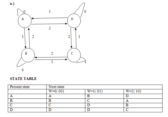
Class 37 1. The state diagram below is designed to output four values in sequence according to the following rules: W-2 passes through the sequence at double-speed, W-1 passes through the sequenc...
P6 (15 points): The FSM state diagram below has two inputs x1 and xo In addition,...
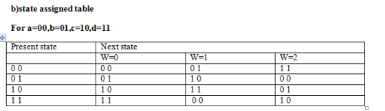
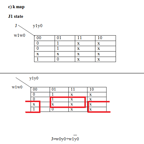
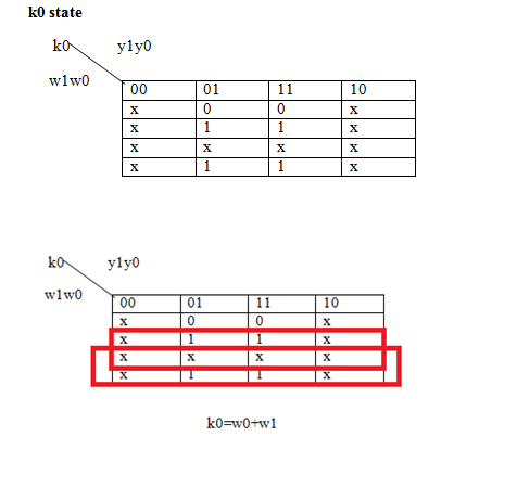
 P6 (15 points): The FSM state diagram below has two inputs x1 and xo In addition, it has two DFFS, three 4-to-1 MUXes, a single XOR gate, a single AND gate, and a single output bit Z. Answer the following questions about this FSM. o/0 10/0 RESET A 61/0 C 9/0 01/0 1/0 o1/0 6/0 A: Is this a Moore FSM or a Mealy FSM? B: The state encodings are A-00, B-01, C-10, and D=11. Write a state- assigned table...
1. Given the state diagram shown below for a state machine with one-bit input W and two-bit outpu...
 1. Given the state diagram shown below for a state machine with
one-bit input W and two-bit output Z:
a. (20 points) Using the state assignments below, make the
state-assigned table. Let S0 = 001, S1 = 010, and S2 = 100.
b. (20 points) Let the state variables be Y2, Y1, and Y0. Derive
an expression for each of the next state variables.
c. (10 points) Derive expressions for the output of this state
diagram.
d. (20 points) Draw...
1. Given the state diagram shown below for a state machine with
one-bit input W and two-bit output Z:
a. (20 points) Using the state assignments below, make the
state-assigned table. Let S0 = 001, S1 = 010, and S2 = 100.
b. (20 points) Let the state variables be Y2, Y1, and Y0. Derive
an expression for each of the next state variables.
c. (10 points) Derive expressions for the output of this state
diagram.
d. (20 points) Draw...
EEL3712 Logic Design Fall 2017 page 3 1. (11pts-2+2+2+3+2 (bonus)) Solve the following questions. a) Build...
 EEL3712 Logic Design Fall 2017 page 3 1. (11pts-2+2+2+3+2 (bonus)) Solve the following questions. a) Build a 8-to-1 MUX from a number of 2-to-1 MUX(S) only. Please also give the logic equation for the 8-t0-1 MUX that you made. b) Build a 6-to-1 MUX from a number of 2-to-1 MUX(s) only. Please also give the logic equation for the 6-to-1 MUX that you designed. c) Please write the Boolean equation of a two input XOR gate, and then use only...
SEQUENCE is 101 In Lab Procedure 1. Draw the state diagram of the state machine below...
 SEQUENCE is 101
In Lab Procedure
1. Draw the state diagram of the state machine below and show it
to the lab instructor.
2. Fill the state table.
3. Assign State numbers
4. Find simplified Expressions (State Equations) for the
flip-flops
5. Draw the circuit diagram using NAND GATES ONLY for the state
machine
STATE DIAGRAM::
STATE TABLE::
State Table Next State Qc Y DA DB Dc Present State QA Qв 0 0 0 0 0 0 0 0 0...
SEQUENCE is 101
In Lab Procedure
1. Draw the state diagram of the state machine below and show it
to the lab instructor.
2. Fill the state table.
3. Assign State numbers
4. Find simplified Expressions (State Equations) for the
flip-flops
5. Draw the circuit diagram using NAND GATES ONLY for the state
machine
STATE DIAGRAM::
STATE TABLE::
State Table Next State Qc Y DA DB Dc Present State QA Qв 0 0 0 0 0 0 0 0 0...
14. Design a cyclic counter that produces the binary sequence 0, 2, 3,1. o..if the control signal...
 14?
14. Design a cyclic counter that produces the binary sequence 0, 2, 3,1. o..if the control signal X is 0 but produces the binary sequence 0, 1,3,2.0, if the control signal X is1.Use D flip-flops. (a) Draw the state diagram; (6 points (b) Draw the input, present state-next state, excitation table: (6 points) (c) Derive the minimal SOP expressions for the D inputs of the flip-flops using K-maps. Draw the logic circuit realization of the counter, using only NAND...
14?
14. Design a cyclic counter that produces the binary sequence 0, 2, 3,1. o..if the control signal X is 0 but produces the binary sequence 0, 1,3,2.0, if the control signal X is1.Use D flip-flops. (a) Draw the state diagram; (6 points (b) Draw the input, present state-next state, excitation table: (6 points) (c) Derive the minimal SOP expressions for the D inputs of the flip-flops using K-maps. Draw the logic circuit realization of the counter, using only NAND...
4. (30 pts.) Construct an asynchronous sequential dual edge trigger circuit which at each change (0 1 or 10) of the inp...
 4. (30 pts.) Construct an asynchronous sequential dual edge trigger circuit which at each change (0 1 or 10) of the input signal w generates a short pulse at the output z. When the input signal is unchanged, the output should be z 0. Output pulse length is given by the time for the transition state in the asynchronous sequential circuit. See timing diagram for clarification. Your answer must include a state diagram, if necessary minimized, a flow table, and...
Thc state transition table bclow is for a sequential circuit with onc input X and onc output Y. The circuit has two state variables A and B, and synchronous input Reset that resets the circuit to sta...
 Thc state transition table bclow is for a sequential circuit with onc input X and onc output Y. The circuit has two state variables A and B, and synchronous input Reset that resets the circuit to state AB-01 when Reset 1: Present State Next State Output X-0 A B A B 0 Reset State 0 0 (9 points) Implement the sequential circuit using minimum number of logic gates and rising- edge triggered D-FFs and draw the logic diagram of the...
NAND Problem 3 (30 points) Consider the circuit shown alongside. Notice that there is one A input...
 NAND Problem 3 (30 points) Consider the circuit shown alongside. Notice that there is one A input x and one output. FULL ADDER XOR (a) [5 points] Determine the B Q Cout Clk flip-flop input equations and xin the output z in terms of the present states A, B and input variable x in other words 4-1 compute T, J, K and z. MUX (b) [10 points] Use the above 1 equations to derive the state- 01 table. Assume the...
show work plz Consider the following finite state diagram. State 1 Output=1 State 0 Output=0 State...
 show work plz
Consider the following finite state diagram. State 1 Output=1 State 0 Output=0 State 2 Output=1 State 3 Output=0 The diagram has 4 states, 1 external input / (in additional to the CLK input), and 1 output bit Y. State 0 is represented by memory bits Qi Qo=00, State 1 is represented by memory bits Q.Qo=01, State 2 is represented by memory bits Q.Qo = 10, and State 3 is represented by memory bits Q.Qo = 11. The...
show work plz
Consider the following finite state diagram. State 1 Output=1 State 0 Output=0 State 2 Output=1 State 3 Output=0 The diagram has 4 states, 1 external input / (in additional to the CLK input), and 1 output bit Y. State 0 is represented by memory bits Qi Qo=00, State 1 is represented by memory bits Q.Qo=01, State 2 is represented by memory bits Q.Qo = 10, and State 3 is represented by memory bits Q.Qo = 11. The...
3. Implement the following gates using only one TTLİCİ (1 point) TEL EL (a) Example: One...
 3. Implement the following gates using only one TTLİCİ (1 point) TEL EL (a) Example: One 4-input OR gate (b) One 2-input NAND gate and one 2-input OR gate (c) One inverter, one 2-input NAND and one 3-input NAND (d) One 2-input XOR gate and one 2-input XNOR (e) One 4-input XNOR gate 2346 GND 2-input OR 7432 1 Porcuits Simplify the following expressions, and implement them with two-level NAND gate circuits: 4. Minterms, K-map and two-level NAND/NAND logic: F...
 P6 (15 points): The FSM state diagram below has two inputs x1 and xo In addition, it has two DFFS, three 4-to-1 MUXes, a single XOR gate, a single AND gate, and a single output bit Z. Answer the following questions about this FSM. o/0 10/0 RESET A 61/0 C 9/0 01/0 1/0 o1/0 6/0 A: Is this a Moore FSM or a Mealy FSM? B: The state encodings are A-00, B-01, C-10, and D=11. Write a state- assigned table...
 1. Given the state diagram shown below for a state machine with
one-bit input W and two-bit output Z:
a. (20 points) Using the state assignments below, make the
state-assigned table. Let S0 = 001, S1 = 010, and S2 = 100.
b. (20 points) Let the state variables be Y2, Y1, and Y0. Derive
an expression for each of the next state variables.
c. (10 points) Derive expressions for the output of this state
diagram.
d. (20 points) Draw...
1. Given the state diagram shown below for a state machine with
one-bit input W and two-bit output Z:
a. (20 points) Using the state assignments below, make the
state-assigned table. Let S0 = 001, S1 = 010, and S2 = 100.
b. (20 points) Let the state variables be Y2, Y1, and Y0. Derive
an expression for each of the next state variables.
c. (10 points) Derive expressions for the output of this state
diagram.
d. (20 points) Draw...
 EEL3712 Logic Design Fall 2017 page 3 1. (11pts-2+2+2+3+2 (bonus)) Solve the following questions. a) Build a 8-to-1 MUX from a number of 2-to-1 MUX(S) only. Please also give the logic equation for the 8-t0-1 MUX that you made. b) Build a 6-to-1 MUX from a number of 2-to-1 MUX(s) only. Please also give the logic equation for the 6-to-1 MUX that you designed. c) Please write the Boolean equation of a two input XOR gate, and then use only...
 SEQUENCE is 101
In Lab Procedure
1. Draw the state diagram of the state machine below and show it
to the lab instructor.
2. Fill the state table.
3. Assign State numbers
4. Find simplified Expressions (State Equations) for the
flip-flops
5. Draw the circuit diagram using NAND GATES ONLY for the state
machine
STATE DIAGRAM::
STATE TABLE::
State Table Next State Qc Y DA DB Dc Present State QA Qв 0 0 0 0 0 0 0 0 0...
SEQUENCE is 101
In Lab Procedure
1. Draw the state diagram of the state machine below and show it
to the lab instructor.
2. Fill the state table.
3. Assign State numbers
4. Find simplified Expressions (State Equations) for the
flip-flops
5. Draw the circuit diagram using NAND GATES ONLY for the state
machine
STATE DIAGRAM::
STATE TABLE::
State Table Next State Qc Y DA DB Dc Present State QA Qв 0 0 0 0 0 0 0 0 0...
 14?
14. Design a cyclic counter that produces the binary sequence 0, 2, 3,1. o..if the control signal X is 0 but produces the binary sequence 0, 1,3,2.0, if the control signal X is1.Use D flip-flops. (a) Draw the state diagram; (6 points (b) Draw the input, present state-next state, excitation table: (6 points) (c) Derive the minimal SOP expressions for the D inputs of the flip-flops using K-maps. Draw the logic circuit realization of the counter, using only NAND...
14?
14. Design a cyclic counter that produces the binary sequence 0, 2, 3,1. o..if the control signal X is 0 but produces the binary sequence 0, 1,3,2.0, if the control signal X is1.Use D flip-flops. (a) Draw the state diagram; (6 points (b) Draw the input, present state-next state, excitation table: (6 points) (c) Derive the minimal SOP expressions for the D inputs of the flip-flops using K-maps. Draw the logic circuit realization of the counter, using only NAND...
 4. (30 pts.) Construct an asynchronous sequential dual edge trigger circuit which at each change (0 1 or 10) of the input signal w generates a short pulse at the output z. When the input signal is unchanged, the output should be z 0. Output pulse length is given by the time for the transition state in the asynchronous sequential circuit. See timing diagram for clarification. Your answer must include a state diagram, if necessary minimized, a flow table, and...
 Thc state transition table bclow is for a sequential circuit with onc input X and onc output Y. The circuit has two state variables A and B, and synchronous input Reset that resets the circuit to state AB-01 when Reset 1: Present State Next State Output X-0 A B A B 0 Reset State 0 0 (9 points) Implement the sequential circuit using minimum number of logic gates and rising- edge triggered D-FFs and draw the logic diagram of the...
 NAND Problem 3 (30 points) Consider the circuit shown alongside. Notice that there is one A input x and one output. FULL ADDER XOR (a) [5 points] Determine the B Q Cout Clk flip-flop input equations and xin the output z in terms of the present states A, B and input variable x in other words 4-1 compute T, J, K and z. MUX (b) [10 points] Use the above 1 equations to derive the state- 01 table. Assume the...
 show work plz
Consider the following finite state diagram. State 1 Output=1 State 0 Output=0 State 2 Output=1 State 3 Output=0 The diagram has 4 states, 1 external input / (in additional to the CLK input), and 1 output bit Y. State 0 is represented by memory bits Qi Qo=00, State 1 is represented by memory bits Q.Qo=01, State 2 is represented by memory bits Q.Qo = 10, and State 3 is represented by memory bits Q.Qo = 11. The...
show work plz
Consider the following finite state diagram. State 1 Output=1 State 0 Output=0 State 2 Output=1 State 3 Output=0 The diagram has 4 states, 1 external input / (in additional to the CLK input), and 1 output bit Y. State 0 is represented by memory bits Qi Qo=00, State 1 is represented by memory bits Q.Qo=01, State 2 is represented by memory bits Q.Qo = 10, and State 3 is represented by memory bits Q.Qo = 11. The...
 3. Implement the following gates using only one TTLİCİ (1 point) TEL EL (a) Example: One 4-input OR gate (b) One 2-input NAND gate and one 2-input OR gate (c) One inverter, one 2-input NAND and one 3-input NAND (d) One 2-input XOR gate and one 2-input XNOR (e) One 4-input XNOR gate 2346 GND 2-input OR 7432 1 Porcuits Simplify the following expressions, and implement them with two-level NAND gate circuits: 4. Minterms, K-map and two-level NAND/NAND logic: F...
Most questions answered within 3 hours.
-
Identify and describe in detail the four categories of
institutions that could be included in a...
asked 1 minute ago -
In python
class Customer:
def __init__(self, customer_id, last_name, first_name, phone_number, address):
self._customer_id = int(customer_id)
self._last_name =...
asked 9 minutes ago -
What is an example of a limitation in implementing a new
ERP system and how it...
asked 4 minutes ago -
In a section of 9.7cm of an artery with a radius of 2.6mm there
is a...
asked 5 minutes ago -
the two carboxylic acid groups of aspartic acid have different
acidities with pKa values of 2.1...
asked 9 minutes ago -
Would CuCO3 aqueous salt combined with calcium chloride
form a solid precipitate? If so, what would...
asked 8 minutes ago -
How do ECM Solutions assist in embedding a culture of continuous
improvement in an organization? (Project...
asked 28 minutes ago -
Directions
These directions introduce the idea of Essential Questions.
Since this may be a new concept...
asked 30 minutes ago -
1.b. Fiscal policy is said to suffer from ‘crowding out’.
Explain what this means and why...
asked 48 minutes ago -
The equation for the reaction of nitrogen and oxygen to form
nitrogen oxide is written as...
asked 52 minutes ago -
A scientist reproducing some photoelectric effect experiments
shines a light on a metal electrode, but doesn't...
asked 55 minutes ago -
In a study designed to test the effectiveness of magnets for
treating back pain, 35 patients...
asked 1 hour ago