![a) For the combination network of JFET and BJT in Fig. 4, determine the following parameters: Ib, Ip, Vgs, V [6.0 marks] VCC](http://img.homeworklib.com/questions/c9709a90-04e6-11eb-96b9-53b5fe7b5e3a.png?x-oss-process=image/resize,w_560)
Homework Answers


Add Answer to:
a) For the combination network of JFET and BJT in Fig. 4, determine the following parameters:...
10) Calculate the voltage at the drain of the JFET in this combination network. O +16...
 10) Calculate the voltage at the drain of the JFET in this combination network. O +16 V 85 k2 > 2.1 ko LoVout loss = 10 mA Vos = -7 V -O VC 2 M2 w B = 120 25 ko 16ko A) Vp = 8.22 V B) VD -3.5V D) Vp - 12.58 V c) Vp - 4.14 V electro electronic circuits itt ettronici
please choose one of the answer choices above. Must show all work, thank you Question 1...
 please choose one of the answer choices above.
Must show all work, thank you
Question 1 CIRCUIT A.1 (2.5 Marks) + Vcc RB IB Rc Vc VB Fig. 1: CIRCUIT A.1 Statement: Sketching relevant output (Vc-Ic) characteristics decide on Q-point coordinates and DC load-line details: That is, determine DC operating conditions of the NPN-BJT/Si circuit of Fig.1 (denoting the type Circuit A1). Assume the following: Vcc= 12 volt; Rc = 3.6 k; RB = 500 k and a = 0.9....
please choose one of the answer choices above.
Must show all work, thank you
Question 1 CIRCUIT A.1 (2.5 Marks) + Vcc RB IB Rc Vc VB Fig. 1: CIRCUIT A.1 Statement: Sketching relevant output (Vc-Ic) characteristics decide on Q-point coordinates and DC load-line details: That is, determine DC operating conditions of the NPN-BJT/Si circuit of Fig.1 (denoting the type Circuit A1). Assume the following: Vcc= 12 volt; Rc = 3.6 k; RB = 500 k and a = 0.9....
please choose one of the answer choices above. Must show all work, thank you Question 4...
 please choose one of the answer choices above.
Must show all work, thank you
Question 4 CIRCUIT B2 (2.5 Marks) +Vcc Rc IRC Vic RB Ів Vc VB VE RE IE FIG.4: CIRCUIT B2 Statement: Sketching relevant output (Vc-Ic) characteristics decide on Q-point coordinates and DC load-line details: That is, determine DC operating conditions of the NPN-BJT/Si circuit of Fig.4 (denoting the type Circuit B2). Assume the following: Vcc= 24 volt; Rc = 5.0 k; RE = 1000 ohm; RB...
please choose one of the answer choices above.
Must show all work, thank you
Question 4 CIRCUIT B2 (2.5 Marks) +Vcc Rc IRC Vic RB Ів Vc VB VE RE IE FIG.4: CIRCUIT B2 Statement: Sketching relevant output (Vc-Ic) characteristics decide on Q-point coordinates and DC load-line details: That is, determine DC operating conditions of the NPN-BJT/Si circuit of Fig.4 (denoting the type Circuit B2). Assume the following: Vcc= 24 volt; Rc = 5.0 k; RE = 1000 ohm; RB...
4. Lab VIII: Experiment VII The Bipolar Junction Transistor (BJT) Characteristics The bipolar junction transistor (BJT)...
 4. Lab VIII: Experiment VII The Bipolar Junction Transistor (BJT) Characteristics The bipolar junction transistor (BJT) is a three-terminal solid state device widely used as an amplifier (or switching) device. It consists of two n-type materials sandwiched by p-type material (npn) or two p-type and n-type. The terminals (sections) are known as emitter E, base B and collector C. Two currents and two voltages uniquely describe the behavior of the device. The third current/voltage can be determined through KCL/KVL. See...
please choose one of the answer choices above. Must show all work, thank you Question 5...
 please choose one of the answer choices above.
Must show all work, thank you
Question 5 CIRCUIT C1 (2.5 Marks) Statement: Sketching relevant output (Vc-Ic) characteristics decide on Q-point coordinates and DC load-line details: That is, determine DC operating conditions of the NPN-BJT/Si circuit of Fig.5 (denoting the type Circuit C1). Assume the following: Vcc= 18 volt; Rc = 1.5 k; RB1 = 75 k; RB2 = 3.6 k; V CESat = 1 volt; and a = 0.99338. +Vcc VIC...
please choose one of the answer choices above.
Must show all work, thank you
Question 5 CIRCUIT C1 (2.5 Marks) Statement: Sketching relevant output (Vc-Ic) characteristics decide on Q-point coordinates and DC load-line details: That is, determine DC operating conditions of the NPN-BJT/Si circuit of Fig.5 (denoting the type Circuit C1). Assume the following: Vcc= 18 volt; Rc = 1.5 k; RB1 = 75 k; RB2 = 3.6 k; V CESat = 1 volt; and a = 0.99338. +Vcc VIC...
#4 The accompanying circuit shows a 4-resistor biased JFET transistor Determine the values of Rp and Rs so that the Q-point is equal to, VDsq 10 V and IDg 5 mA . For the JFET take IDss = 10 mA...
 #4
The accompanying circuit shows a 4-resistor biased JFET transistor Determine the values of Rp and Rs so that the Q-point is equal to, VDsq 10 V and IDg 5 mA . For the JFET take IDss = 10 mA, VP =-5 V and λ 0 . The circuit parameters are, R1-740 k, R2-22 1.85 ka, Rs-85 ㏀ and RL-3.5 ㏀. Take the power supply VDD 24 V 2- Vo R1 Vi R2 Signal generator 4-In reference to the circuit...
#4
The accompanying circuit shows a 4-resistor biased JFET transistor Determine the values of Rp and Rs so that the Q-point is equal to, VDsq 10 V and IDg 5 mA . For the JFET take IDss = 10 mA, VP =-5 V and λ 0 . The circuit parameters are, R1-740 k, R2-22 1.85 ka, Rs-85 ㏀ and RL-3.5 ㏀. Take the power supply VDD 24 V 2- Vo R1 Vi R2 Signal generator 4-In reference to the circuit...
please choose one of the answer choices above. Must show all work, thank you Question 3...
 please choose one of the answer choices above.
Must show all work, thank you
Question 3 CIRCUIT B1 (2.5 Marks) + Vcc Rc IRC > IC RB Ів + VCE IE FIG. 3: CIRCUIT B1 Statement: Sketching relevant output (Vc-Ic) characteristics decide on Q-point coordinates and DC load-line details: That is, determine DC operating conditions of the NPN-BJT/Si circuit of Fig.3 (denoting the type Circuit B1). Assume the following: Vcc= 20 volt; Rc = 2.5 k; RB = 350 k...
please choose one of the answer choices above.
Must show all work, thank you
Question 3 CIRCUIT B1 (2.5 Marks) + Vcc Rc IRC > IC RB Ів + VCE IE FIG. 3: CIRCUIT B1 Statement: Sketching relevant output (Vc-Ic) characteristics decide on Q-point coordinates and DC load-line details: That is, determine DC operating conditions of the NPN-BJT/Si circuit of Fig.3 (denoting the type Circuit B1). Assume the following: Vcc= 20 volt; Rc = 2.5 k; RB = 350 k...
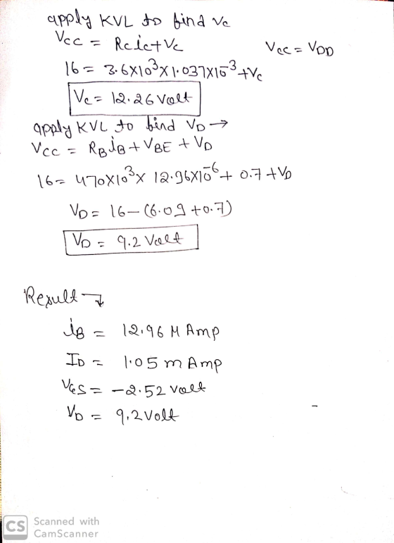
Problem 4 (20 %) For the circuit shown in Figure 4 determine IB, IC, and VC....
 Problem 4 (20 %) For the circuit shown in Figure 4 determine IB,
IC, and VC. Data VCC=9 V VBB=4 V R2= 165 k R1= 2.5 k Transistor
Assume VBE ≈ 0.7 V and =150
Derive all the results. Give the answers with the preestablished
prefix.
FAVOR DIBUJAR LOS CIRCUITOS
Problem 4 (206) For the circuit shown in Figure 4 determine IB, I, and Vc. Data Ve=9 V V=4V R = 165 kg R=2.5k_2 Transistor Assume VE 0.7 V and...
Problem 4 (20 %) For the circuit shown in Figure 4 determine IB,
IC, and VC. Data VCC=9 V VBB=4 V R2= 165 k R1= 2.5 k Transistor
Assume VBE ≈ 0.7 V and =150
Derive all the results. Give the answers with the preestablished
prefix.
FAVOR DIBUJAR LOS CIRCUITOS
Problem 4 (206) For the circuit shown in Figure 4 determine IB, I, and Vc. Data Ve=9 V V=4V R = 165 kg R=2.5k_2 Transistor Assume VE 0.7 V and...
Electronics1. It's a multiple choices question. use the formula sheet if needed (the last picture). Question...
 Electronics1. It's a multiple choices question. use the formula
sheet if needed (the last picture).
Question 3 CIRCUIT B1 (2.5 Marks) + VC Rc IRC < + RB IC IB V ce → IE FIG. 3: CIRCUIT B1 Statement: Sketching relevant output (V-Ic) characteristics decide on Q-point coordinates and DC load-line details: That is, determine DC operating conditions of the NPN-BJT/Si circuit of Fig.3 (denoting the type Circuit B1). Assume the following: Vcc= 20 volt; Rc = 2.5 k; RB...
Electronics1. It's a multiple choices question. use the formula
sheet if needed (the last picture).
Question 3 CIRCUIT B1 (2.5 Marks) + VC Rc IRC < + RB IC IB V ce → IE FIG. 3: CIRCUIT B1 Statement: Sketching relevant output (V-Ic) characteristics decide on Q-point coordinates and DC load-line details: That is, determine DC operating conditions of the NPN-BJT/Si circuit of Fig.3 (denoting the type Circuit B1). Assume the following: Vcc= 20 volt; Rc = 2.5 k; RB...
A common-emitter BJT amplificr is shown in Fig.8.1. Note the DC biasing values and the BJTsmall-s...
 A common-emitter BJT amplificr is shown in Fig.8.1. Note the DC biasing values and the BJTsmall-signalmodel parameters from the class-signment #9 on DC Bia ing. Neglect the value of Rs in your calculations, k1 Rs-a k2: 1· Cal ulatethesmall-agalpannetas ofthe amplifi randcompletethecalculated valuesinTable8-1 Smalls-signal voltage gai, AVk Small-signal input resistance,k, Small-signaloutput resistance, Ro VW RC 2k C2 RB 570k Rs C1 1 10uP 0.1m 1 Vs CE RE 2k SINE(0 1mV 1kHz 0 0 00) tran 0 2ms 0 1us...
 10) Calculate the voltage at the drain of the JFET in this combination network. O +16 V 85 k2 > 2.1 ko LoVout loss = 10 mA Vos = -7 V -O VC 2 M2 w B = 120 25 ko 16ko A) Vp = 8.22 V B) VD -3.5V D) Vp - 12.58 V c) Vp - 4.14 V electro electronic circuits itt ettronici
 please choose one of the answer choices above.
Must show all work, thank you
Question 1 CIRCUIT A.1 (2.5 Marks) + Vcc RB IB Rc Vc VB Fig. 1: CIRCUIT A.1 Statement: Sketching relevant output (Vc-Ic) characteristics decide on Q-point coordinates and DC load-line details: That is, determine DC operating conditions of the NPN-BJT/Si circuit of Fig.1 (denoting the type Circuit A1). Assume the following: Vcc= 12 volt; Rc = 3.6 k; RB = 500 k and a = 0.9....
please choose one of the answer choices above.
Must show all work, thank you
Question 1 CIRCUIT A.1 (2.5 Marks) + Vcc RB IB Rc Vc VB Fig. 1: CIRCUIT A.1 Statement: Sketching relevant output (Vc-Ic) characteristics decide on Q-point coordinates and DC load-line details: That is, determine DC operating conditions of the NPN-BJT/Si circuit of Fig.1 (denoting the type Circuit A1). Assume the following: Vcc= 12 volt; Rc = 3.6 k; RB = 500 k and a = 0.9....
 please choose one of the answer choices above.
Must show all work, thank you
Question 4 CIRCUIT B2 (2.5 Marks) +Vcc Rc IRC Vic RB Ів Vc VB VE RE IE FIG.4: CIRCUIT B2 Statement: Sketching relevant output (Vc-Ic) characteristics decide on Q-point coordinates and DC load-line details: That is, determine DC operating conditions of the NPN-BJT/Si circuit of Fig.4 (denoting the type Circuit B2). Assume the following: Vcc= 24 volt; Rc = 5.0 k; RE = 1000 ohm; RB...
please choose one of the answer choices above.
Must show all work, thank you
Question 4 CIRCUIT B2 (2.5 Marks) +Vcc Rc IRC Vic RB Ів Vc VB VE RE IE FIG.4: CIRCUIT B2 Statement: Sketching relevant output (Vc-Ic) characteristics decide on Q-point coordinates and DC load-line details: That is, determine DC operating conditions of the NPN-BJT/Si circuit of Fig.4 (denoting the type Circuit B2). Assume the following: Vcc= 24 volt; Rc = 5.0 k; RE = 1000 ohm; RB...
 4. Lab VIII: Experiment VII The Bipolar Junction Transistor (BJT) Characteristics The bipolar junction transistor (BJT) is a three-terminal solid state device widely used as an amplifier (or switching) device. It consists of two n-type materials sandwiched by p-type material (npn) or two p-type and n-type. The terminals (sections) are known as emitter E, base B and collector C. Two currents and two voltages uniquely describe the behavior of the device. The third current/voltage can be determined through KCL/KVL. See...
 please choose one of the answer choices above.
Must show all work, thank you
Question 5 CIRCUIT C1 (2.5 Marks) Statement: Sketching relevant output (Vc-Ic) characteristics decide on Q-point coordinates and DC load-line details: That is, determine DC operating conditions of the NPN-BJT/Si circuit of Fig.5 (denoting the type Circuit C1). Assume the following: Vcc= 18 volt; Rc = 1.5 k; RB1 = 75 k; RB2 = 3.6 k; V CESat = 1 volt; and a = 0.99338. +Vcc VIC...
please choose one of the answer choices above.
Must show all work, thank you
Question 5 CIRCUIT C1 (2.5 Marks) Statement: Sketching relevant output (Vc-Ic) characteristics decide on Q-point coordinates and DC load-line details: That is, determine DC operating conditions of the NPN-BJT/Si circuit of Fig.5 (denoting the type Circuit C1). Assume the following: Vcc= 18 volt; Rc = 1.5 k; RB1 = 75 k; RB2 = 3.6 k; V CESat = 1 volt; and a = 0.99338. +Vcc VIC...
 #4
The accompanying circuit shows a 4-resistor biased JFET transistor Determine the values of Rp and Rs so that the Q-point is equal to, VDsq 10 V and IDg 5 mA . For the JFET take IDss = 10 mA, VP =-5 V and λ 0 . The circuit parameters are, R1-740 k, R2-22 1.85 ka, Rs-85 ㏀ and RL-3.5 ㏀. Take the power supply VDD 24 V 2- Vo R1 Vi R2 Signal generator 4-In reference to the circuit...
#4
The accompanying circuit shows a 4-resistor biased JFET transistor Determine the values of Rp and Rs so that the Q-point is equal to, VDsq 10 V and IDg 5 mA . For the JFET take IDss = 10 mA, VP =-5 V and λ 0 . The circuit parameters are, R1-740 k, R2-22 1.85 ka, Rs-85 ㏀ and RL-3.5 ㏀. Take the power supply VDD 24 V 2- Vo R1 Vi R2 Signal generator 4-In reference to the circuit...
 please choose one of the answer choices above.
Must show all work, thank you
Question 3 CIRCUIT B1 (2.5 Marks) + Vcc Rc IRC > IC RB Ів + VCE IE FIG. 3: CIRCUIT B1 Statement: Sketching relevant output (Vc-Ic) characteristics decide on Q-point coordinates and DC load-line details: That is, determine DC operating conditions of the NPN-BJT/Si circuit of Fig.3 (denoting the type Circuit B1). Assume the following: Vcc= 20 volt; Rc = 2.5 k; RB = 350 k...
please choose one of the answer choices above.
Must show all work, thank you
Question 3 CIRCUIT B1 (2.5 Marks) + Vcc Rc IRC > IC RB Ів + VCE IE FIG. 3: CIRCUIT B1 Statement: Sketching relevant output (Vc-Ic) characteristics decide on Q-point coordinates and DC load-line details: That is, determine DC operating conditions of the NPN-BJT/Si circuit of Fig.3 (denoting the type Circuit B1). Assume the following: Vcc= 20 volt; Rc = 2.5 k; RB = 350 k...
 Problem 4 (20 %) For the circuit shown in Figure 4 determine IB,
IC, and VC. Data VCC=9 V VBB=4 V R2= 165 k R1= 2.5 k Transistor
Assume VBE ≈ 0.7 V and =150
Derive all the results. Give the answers with the preestablished
prefix.
FAVOR DIBUJAR LOS CIRCUITOS
Problem 4 (206) For the circuit shown in Figure 4 determine IB, I, and Vc. Data Ve=9 V V=4V R = 165 kg R=2.5k_2 Transistor Assume VE 0.7 V and...
Problem 4 (20 %) For the circuit shown in Figure 4 determine IB,
IC, and VC. Data VCC=9 V VBB=4 V R2= 165 k R1= 2.5 k Transistor
Assume VBE ≈ 0.7 V and =150
Derive all the results. Give the answers with the preestablished
prefix.
FAVOR DIBUJAR LOS CIRCUITOS
Problem 4 (206) For the circuit shown in Figure 4 determine IB, I, and Vc. Data Ve=9 V V=4V R = 165 kg R=2.5k_2 Transistor Assume VE 0.7 V and...
 Electronics1. It's a multiple choices question. use the formula
sheet if needed (the last picture).
Question 3 CIRCUIT B1 (2.5 Marks) + VC Rc IRC < + RB IC IB V ce → IE FIG. 3: CIRCUIT B1 Statement: Sketching relevant output (V-Ic) characteristics decide on Q-point coordinates and DC load-line details: That is, determine DC operating conditions of the NPN-BJT/Si circuit of Fig.3 (denoting the type Circuit B1). Assume the following: Vcc= 20 volt; Rc = 2.5 k; RB...
Electronics1. It's a multiple choices question. use the formula
sheet if needed (the last picture).
Question 3 CIRCUIT B1 (2.5 Marks) + VC Rc IRC < + RB IC IB V ce → IE FIG. 3: CIRCUIT B1 Statement: Sketching relevant output (V-Ic) characteristics decide on Q-point coordinates and DC load-line details: That is, determine DC operating conditions of the NPN-BJT/Si circuit of Fig.3 (denoting the type Circuit B1). Assume the following: Vcc= 20 volt; Rc = 2.5 k; RB...
 A common-emitter BJT amplificr is shown in Fig.8.1. Note the DC biasing values and the BJTsmall-signalmodel parameters from the class-signment #9 on DC Bia ing. Neglect the value of Rs in your calculations, k1 Rs-a k2: 1· Cal ulatethesmall-agalpannetas ofthe amplifi randcompletethecalculated valuesinTable8-1 Smalls-signal voltage gai, AVk Small-signal input resistance,k, Small-signaloutput resistance, Ro VW RC 2k C2 RB 570k Rs C1 1 10uP 0.1m 1 Vs CE RE 2k SINE(0 1mV 1kHz 0 0 00) tran 0 2ms 0 1us...
Most questions answered within 3 hours.
-
Two concentric current loops lie in the same plane. The smaller
loop has a radius of...
asked 24 minutes ago -
1)Which of the following is an
important difference between qualified and nonqualified retirement
plans?
a. Qualified...
asked 36 minutes ago -
What's the streaming business's problem on the
horizon?
asked 1 hour ago -
I need help with writing the conclusion for this online lab
report
Abstract
By testing the...
asked 1 hour ago -
For the reaction 1N2+3H2-----> 2NH3, would the reaction rate
trend be: delta[NH3]/ delta t = -2...
asked 2 hours ago -
Within your current/past organization, identify a problem/issue
and format a design to address same. You may...
asked 2 hours ago -
A sock stuck to the side of a clothes-dryer barrel has a
centripetal acceleration of 24...
asked 3 hours ago -
A perfect gas undergoes an isentropic process such that its
volume doubles. If the ratio of...
asked 3 hours ago -
list the elements in groups 3A to 6A in the same order as in the
periodic...
asked 3 hours ago -
Estimating effect size. Peng and Chen (2014)
evaluated effect size estimates for various tests. In their...
asked 3 hours ago -
Write a script in MySQL that creates and calls a stored
procedure name test. This procedure...
asked 3 hours ago -
If we test the following: H0: μ = 17
vs. H1: μ ≠ 17 and the...
asked 3 hours ago