The figure below shows an address decoder used to select between four memory mapped components connected to a microprocessor with a 24-bit address bus.
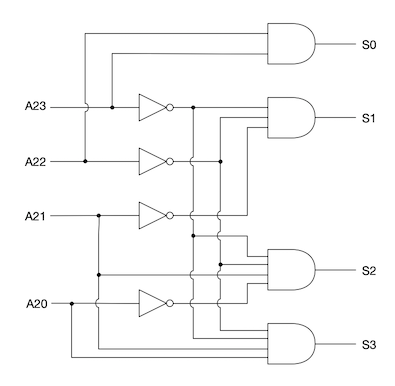
What is the size of the processor address space? (Justify your answer.)
Homework Answers

Add Answer to:
The figure below shows an address decoder used to select between
four memory mapped components connected...
The following figure shows the address that is going from a certain processor to a direct-mapped...
 The following figure shows the address that is going
from a certain processor to a direct-mapped cache. The address is
divided into fields. The index of the first bit and the last bit of
each field is written below it. Calculate the size of the data that
is stored in the cache, in Kibytes, and the total number of bits
within the cache, in Kibits.
TAG = 31 - 16
INDEX = 15 - 6
BLOCK OFFSET = 5 -...
The following figure shows the address that is going
from a certain processor to a direct-mapped cache. The address is
divided into fields. The index of the first bit and the last bit of
each field is written below it. Calculate the size of the data that
is stored in the cache, in Kibytes, and the total number of bits
within the cache, in Kibits.
TAG = 31 - 16
INDEX = 15 - 6
BLOCK OFFSET = 5 -...
2) (25 points) Consider a hypothetical mieroprocessor generating 16-bit addresses with 32-bit data accesses (i.e. each access retrieves 32 bits for each address). a. What is the maximum memory ad...
 2) (25 points) Consider a hypothetical mieroprocessor generating 16-bit addresses with 32-bit data accesses (i.e. each access retrieves 32 bits for each address). a. What is the maximum memory address space (i.e., mmber of addresses) that the processor can access directly? What is the maximum memory capacity (in bytes) for this microprocessor? b. c. What is the last memory address that the CPU can access? Write your answer in decimal. What is the maximum memory address space that the processor...
3. (15 Pts.) In this problem you are given a microprocessor with 24-bit address bus and...
 3. (15 Pts.) In this problem you are given a microprocessor with 24-bit address bus and 8-bit data bus. a. What is the addressing space of this microprocessor? 113 16 MB b. how many bytes are contained in the sub-space starting at address C00 000h and ending at address DFF FFFH? Express your answer in KB and MB. DFFFEE CoO DOU - TFFFFF in ke 20 4SKe c. You would like to interface a single 4 MB memory IC to...
Problem #1 (25 points) Address Space, Memory Consider a hypothetical 18-bit processor called HYP18 with all...
 Problem #1 (25 points) Address Space, Memory Consider a hypothetical 18-bit processor called HYP18 with all registers, including PC and SP, being 18 bits long. The smallest addressable unit in memory is an 8-bit byte. A. (4 points) What is the size of HYP18's address space in bytes and KB? How many address lines does HYP18 require? Address space: Bytes Address space: KB (KiloBytes). Address bus lines: B. (6 points) Assume that first quarter of the address space is dedicated...
Explain your reasoning for the following: a) Assume that the 4 x 3 memory given in...
Explain your reasoning for the following: a) Assume that the 4 x 3 memory given in the text book is available in a single chip. How many of these chips are needed to implement a 16x12 memory system? What is the total number of D FFs used for this memory system? b) Find the number of cells in a memory chip that has capacity of 32 Kilobits and is organized as 16-bit cells. How many address and data pins does...
Question 6 For the following figure shows a hypothetical memory hierarchy going from a virtual address to L2 cache acce...
 Question 6 For the following figure shows a hypothetical memory hierarchy going from a virtual address to L2 cache access. The page size is 8KB, the TLB is direct mapped with 128 entries. The L1 cache is a direct mapped 8 KB, and the L2 cache is 2MB and direct mapped. Both use 64 byte blocks. The virtual address is 64 bits and the physical address is 41 bits. For each block in the figure below, fill in the number...
Part RAM - Example 3 Design and all the relevant information for a memory module is...
 Part RAM - Example 3 Design and all the relevant information for a memory module is given in the figure below. Answer the following: (a) What is the size of module M1? 16 (b) What is the size of this memory? (c) If an address (54A3)16 and a read command is issued which memory module will place date on the data bus. M2 dala bus (d) What is the maximum address of any bit in M2. Write your answer in...
you answer for this question but very shortcut can you please answer with some nots thanks . Provide this 8-bit CPU with a 64Kb yte memory space by making use of 16K x 4 memory chip like the ones...
 you answer for this question but very shortcut can you please
answer with some nots thanks
. Provide this 8-bit CPU with a 64Kb yte memory space by making use of 16K x 4 memory chip like the ones provided in the figure below. ) Fill in the blanks beside and inside the memory chips with the appropriate numbers. The number on top of this The spaces besides the A's and the D's are to indicate which lines of the...
you answer for this question but very shortcut can you please
answer with some nots thanks
. Provide this 8-bit CPU with a 64Kb yte memory space by making use of 16K x 4 memory chip like the ones provided in the figure below. ) Fill in the blanks beside and inside the memory chips with the appropriate numbers. The number on top of this The spaces besides the A's and the D's are to indicate which lines of the...
Consider a virtual memory system with the following properties: 36 bit virtual byte address, 8 KB...
Consider a virtual memory system with the following properties: 36 bit virtual byte address, 8 KB pages size, and 32 bit physical byte address. Please explain how you determined your answer. a. What is the size of main memory for this system if all addressable frames are used? b. What is the total size of the page table for each process on this processor, assuming that the valid, protection, dirty, and use bits take a total of 4 bits and...
. An embedded microcontroller with a 20‐bit address bus implements the following four blocks of memory....
 . An embedded microcontroller with a 20‐bit address bus
implements the following four blocks of memory. Draw an address
decoding table to satisfy the following memory map and design an
address decoder to select each of these devices.
a. RAM1 0 0000 ‐ 3 FFFF
b. RAM2 4 0000 ‐ 7 FFFF
c. ROM1 E 0000 ‐ E 7FFF
d. ROM2 F 0000 ‐ F FFFF
I know that the answer is:
I was wondering if someone could explain how...
. An embedded microcontroller with a 20‐bit address bus
implements the following four blocks of memory. Draw an address
decoding table to satisfy the following memory map and design an
address decoder to select each of these devices.
a. RAM1 0 0000 ‐ 3 FFFF
b. RAM2 4 0000 ‐ 7 FFFF
c. ROM1 E 0000 ‐ E 7FFF
d. ROM2 F 0000 ‐ F FFFF
I know that the answer is:
I was wondering if someone could explain how...
 The following figure shows the address that is going
from a certain processor to a direct-mapped cache. The address is
divided into fields. The index of the first bit and the last bit of
each field is written below it. Calculate the size of the data that
is stored in the cache, in Kibytes, and the total number of bits
within the cache, in Kibits.
TAG = 31 - 16
INDEX = 15 - 6
BLOCK OFFSET = 5 -...
The following figure shows the address that is going
from a certain processor to a direct-mapped cache. The address is
divided into fields. The index of the first bit and the last bit of
each field is written below it. Calculate the size of the data that
is stored in the cache, in Kibytes, and the total number of bits
within the cache, in Kibits.
TAG = 31 - 16
INDEX = 15 - 6
BLOCK OFFSET = 5 -...
 2) (25 points) Consider a hypothetical mieroprocessor generating 16-bit addresses with 32-bit data accesses (i.e. each access retrieves 32 bits for each address). a. What is the maximum memory address space (i.e., mmber of addresses) that the processor can access directly? What is the maximum memory capacity (in bytes) for this microprocessor? b. c. What is the last memory address that the CPU can access? Write your answer in decimal. What is the maximum memory address space that the processor...
 3. (15 Pts.) In this problem you are given a microprocessor with 24-bit address bus and 8-bit data bus. a. What is the addressing space of this microprocessor? 113 16 MB b. how many bytes are contained in the sub-space starting at address C00 000h and ending at address DFF FFFH? Express your answer in KB and MB. DFFFEE CoO DOU - TFFFFF in ke 20 4SKe c. You would like to interface a single 4 MB memory IC to...
 Problem #1 (25 points) Address Space, Memory Consider a hypothetical 18-bit processor called HYP18 with all registers, including PC and SP, being 18 bits long. The smallest addressable unit in memory is an 8-bit byte. A. (4 points) What is the size of HYP18's address space in bytes and KB? How many address lines does HYP18 require? Address space: Bytes Address space: KB (KiloBytes). Address bus lines: B. (6 points) Assume that first quarter of the address space is dedicated...
 Question 6 For the following figure shows a hypothetical memory hierarchy going from a virtual address to L2 cache access. The page size is 8KB, the TLB is direct mapped with 128 entries. The L1 cache is a direct mapped 8 KB, and the L2 cache is 2MB and direct mapped. Both use 64 byte blocks. The virtual address is 64 bits and the physical address is 41 bits. For each block in the figure below, fill in the number...
 Part RAM - Example 3 Design and all the relevant information for a memory module is given in the figure below. Answer the following: (a) What is the size of module M1? 16 (b) What is the size of this memory? (c) If an address (54A3)16 and a read command is issued which memory module will place date on the data bus. M2 dala bus (d) What is the maximum address of any bit in M2. Write your answer in...
 you answer for this question but very shortcut can you please
answer with some nots thanks
. Provide this 8-bit CPU with a 64Kb yte memory space by making use of 16K x 4 memory chip like the ones provided in the figure below. ) Fill in the blanks beside and inside the memory chips with the appropriate numbers. The number on top of this The spaces besides the A's and the D's are to indicate which lines of the...
you answer for this question but very shortcut can you please
answer with some nots thanks
. Provide this 8-bit CPU with a 64Kb yte memory space by making use of 16K x 4 memory chip like the ones provided in the figure below. ) Fill in the blanks beside and inside the memory chips with the appropriate numbers. The number on top of this The spaces besides the A's and the D's are to indicate which lines of the...
 . An embedded microcontroller with a 20‐bit address bus
implements the following four blocks of memory. Draw an address
decoding table to satisfy the following memory map and design an
address decoder to select each of these devices.
a. RAM1 0 0000 ‐ 3 FFFF
b. RAM2 4 0000 ‐ 7 FFFF
c. ROM1 E 0000 ‐ E 7FFF
d. ROM2 F 0000 ‐ F FFFF
I know that the answer is:
I was wondering if someone could explain how...
. An embedded microcontroller with a 20‐bit address bus
implements the following four blocks of memory. Draw an address
decoding table to satisfy the following memory map and design an
address decoder to select each of these devices.
a. RAM1 0 0000 ‐ 3 FFFF
b. RAM2 4 0000 ‐ 7 FFFF
c. ROM1 E 0000 ‐ E 7FFF
d. ROM2 F 0000 ‐ F FFFF
I know that the answer is:
I was wondering if someone could explain how...
Most questions answered within 3 hours.
-
In JAVA please (need answers in a few hours!)
Exercise #2: Design and implement a program...
asked 2 hours ago -
The mass spectrum of an organic compound shows the relative
abundances of M to be 53.76%...
asked 3 hours ago -
Coca Cola’s strategy of “think local, act local” represents a
__________ approach.
Question options:
1)
transnational...
asked 3 hours ago -
which of the following is not a category of project management
risk?
a) external
b) internal...
asked 4 hours ago -
Focus on Critical Thinking: Are citizen suit provisions an
effective way to achieve environmental objectives? Do...
asked 5 hours ago -
Gaseous butane CH3CH22CH3 will react with gaseous oxygen O2 to
produce gaseous carbon dioxide CO2 and...
asked 5 hours ago -
Required to construct counters using synchronous sequential
logic. Use one hex digit to display the result....
asked 5 hours ago -
(Ultra) Large-Scale Systems –Characteristics?
explain in detail
How the nature of an enterprise affect complex...
asked 5 hours ago -
Some of the antibiotic susceptible strains show colonies within
the clear zone. What it does this...
asked 6 hours ago -
In the lottery game Fantasy 5 you have to select 5 numbers from
the numbers {1,2,3,.......,38,39}....
asked 6 hours ago -
A call option on Jupiter Motors stock with an exercise price of
$80 and one-year expiration...
asked 6 hours ago -
What is the disadvantage of an automated vulnerability scan tool
like Nessus?
prone to false negatives...
asked 6 hours ago