
Homework Answers

Add Answer to:
Determine the equilibrium electron and hole concentration inside a uniformly doped sample of Si under the...
Assuming complete ionization, determine the equilibrium electron and hole concentrations inside a uniformly doped Si under the following conditions V. Assuming complete ionization, determine the equi...
 Assuming complete ionization, determine the equilibrium electron
and hole concentrations inside a uniformly doped Si under the
following conditions
V. Assuming complete ionization, determine the equilibrium electron and hole concentration inside a uniformly doped Si under the following conditions: a) T= 200 K, N,-9 x 10¹⁵ /cm, ND-1016 /cm3 b) T= 450 K, N,-0, ND-1014 /cm3
V. Assuming complete ionization, determine the equilibrium electron and hole concentration inside a uniformly doped Si under the following conditions: a) T= 200 K,...
Assuming complete ionization, determine the equilibrium electron
and hole concentrations inside a uniformly doped Si under the
following conditions
V. Assuming complete ionization, determine the equilibrium electron and hole concentration inside a uniformly doped Si under the following conditions: a) T= 200 K, N,-9 x 10¹⁵ /cm, ND-1016 /cm3 b) T= 450 K, N,-0, ND-1014 /cm3
V. Assuming complete ionization, determine the equilibrium electron and hole concentration inside a uniformly doped Si under the following conditions: a) T= 200 K,...
Detailed solutions needed, thank you! 5- Determine the equilibrium electron and hole concentrations inside a uniformly...
 Detailed solutions needed, thank you!
5- Determine the equilibrium electron and hole concentrations inside a uniformly doped under the following conditions: (a) Room temperature, NA << ND, ND = 10°/cm ; (b) Room temperature, NA 1016/cm3, ND « NA; (c) Room temperature, NA = 9 x 10¹⁵/cm3, ND = 1016/cm3; (d) T = 450 K, NA = 0, ND = 1014/cm3; (e) T = 650 K, NA = 0, ND = 1014/cm3. sample of Si
Detailed solutions needed, thank you!
5- Determine the equilibrium electron and hole concentrations inside a uniformly doped under the following conditions: (a) Room temperature, NA << ND, ND = 10°/cm ; (b) Room temperature, NA 1016/cm3, ND « NA; (c) Room temperature, NA = 9 x 10¹⁵/cm3, ND = 1016/cm3; (d) T = 450 K, NA = 0, ND = 1014/cm3; (e) T = 650 K, NA = 0, ND = 1014/cm3. sample of Si
2. A GaAs semiconductor at T 300 K is uniformly doped with NA 1016 cm3 and...
 2. A GaAs semiconductor at T 300 K is uniformly doped with NA 1016 cm3 and No 0. The GaAs is illuminated with a light source at t = 0 s, resulting in a uniform generation rate of electron hole pairs g' 1020 cm . The electric field is zero. a) Give the analytic expression for the excess-carrier concentration δn(t) versus the time t>0s b) The steady state excess carrier concentration is found to be on( is the minority carrier...
1. a. Find the main error in each of the band diagrams shown below. For all...
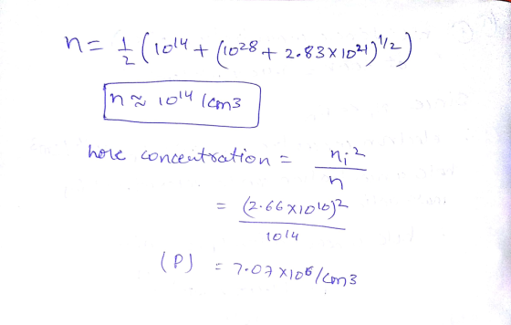
 1. a. Find the main error in each of the band diagrams shown below. For all of the band diagrams Ny 1019/cm3, Ne- 1019/cm3, ni = 3 x 10⁸/cm". E,-1.25 eV, T = 300 K. Ef Ef EFi Main error: Main error: Main error: Main error: Consider a semiconductor sample with the following characteristics: EG 1.25 eV, T 300 K, Nd 5 x 101*/cm3, Na 1014/cm3, N.-1019/cm3, N.-1019/cm3, ni-3 × 10⁸/cm3. Assume complete ionization b. Find the equilibrium electron and...
A Si sample is doped with NA = 5 x 1015cm 3 and optical excited uniformly...
 A Si sample is doped with NA = 5 x 1015cm 3 and optical excited uniformly with gop-1019EHP/cm3,s. As suming T-300K and using carrier lifetime τη-tp-5us and diffusion coefficient D,-35cm2/s and D,- 12.5cm2Is) (a). Find the steady state electron and hole concentrations (n and p) and the separation of their quasi-Fermi levels (Fn Fp). (b). Calculate the of conductivity, σ, of the Si upon illuminating the light
Si sample doped with donors 101°cm-3 initially at room temperature 300 °K (n 31010 cm. Later it i...
 Si sample doped with donors 101°cm-3 initially at room temperature 300 °K (n 31010 cm. Later it is excited optically as such 1019 cm-3electron-hole pairs are produced in one second uniformly in the sample. Si band gap energy isEg-1.11 eV and the recombination for hole electron life-time10 μs. Hint may use results of question 1 above. Draw appropriate figures and mark related levels! a) Calculate the equilibrium Fermi level with respect to conduction band edge Ec b) Calculate the equilibrium...
P4. a. Consider Si doped with P at 2x10^16 cm^-3. determine the carrier concentrations ni, p,...
P4. a. Consider Si doped with P at 2x10^16 cm^-3. determine the carrier concentrations ni, p, and n at T = 300 K. b. Consider a semiconductor with ni = 2.4x10^13cm-3 that is doped such that ND=5x10^13cm^-3. Determine the carrier concentrations n and p. c. Consider a compensation Ge semiconductor with ni = 2.4x10^13 cm^-3 doped at concentration NA=5x10^13 cm^-3. Determine the thermal equilibrium carrier concentration n and p.
14 Q1. Given a NA = 10 /cm" doped Si sample a) b) c) Calculate Ef...
 14 Q1. Given a NA = 10 /cm" doped Si sample a) b) c) Calculate Ef as a function of Temperature T at 500K intervals from 3000K to 5000K. Any conclusion could be drawn from a) part? If the donor has ND-1014/cm3 to replace the NA, what is the Ef at 3000K, 4000K and 5000K The band gap affected by temperature should be included. Q2. At 300K, please find the doping limit of both n-type and p-type Ge to have...
3. An ideal Si pn junction at 300 K is under forward bias. The minority carrier...
 3. An ideal Si pn junction at 300 K is under forward bias. The minority carrier life times are 10* and 107 s for electrons and holes. The doping concentration in the n-region is ND-10° cmPlot the ratio of hole current to the total current crossing the space charge region as the p-region doping concentration (NA varies over the range 1014 to 1018 cnm Use a log scale for the doping concentrations.[use Fig.3.5(a) on P80 for mobility values) 163 cm....
 Assuming complete ionization, determine the equilibrium electron
and hole concentrations inside a uniformly doped Si under the
following conditions
V. Assuming complete ionization, determine the equilibrium electron and hole concentration inside a uniformly doped Si under the following conditions: a) T= 200 K, N,-9 x 10¹⁵ /cm, ND-1016 /cm3 b) T= 450 K, N,-0, ND-1014 /cm3
V. Assuming complete ionization, determine the equilibrium electron and hole concentration inside a uniformly doped Si under the following conditions: a) T= 200 K,...
Assuming complete ionization, determine the equilibrium electron
and hole concentrations inside a uniformly doped Si under the
following conditions
V. Assuming complete ionization, determine the equilibrium electron and hole concentration inside a uniformly doped Si under the following conditions: a) T= 200 K, N,-9 x 10¹⁵ /cm, ND-1016 /cm3 b) T= 450 K, N,-0, ND-1014 /cm3
V. Assuming complete ionization, determine the equilibrium electron and hole concentration inside a uniformly doped Si under the following conditions: a) T= 200 K,...
 Detailed solutions needed, thank you!
5- Determine the equilibrium electron and hole concentrations inside a uniformly doped under the following conditions: (a) Room temperature, NA << ND, ND = 10°/cm ; (b) Room temperature, NA 1016/cm3, ND « NA; (c) Room temperature, NA = 9 x 10¹⁵/cm3, ND = 1016/cm3; (d) T = 450 K, NA = 0, ND = 1014/cm3; (e) T = 650 K, NA = 0, ND = 1014/cm3. sample of Si
Detailed solutions needed, thank you!
5- Determine the equilibrium electron and hole concentrations inside a uniformly doped under the following conditions: (a) Room temperature, NA << ND, ND = 10°/cm ; (b) Room temperature, NA 1016/cm3, ND « NA; (c) Room temperature, NA = 9 x 10¹⁵/cm3, ND = 1016/cm3; (d) T = 450 K, NA = 0, ND = 1014/cm3; (e) T = 650 K, NA = 0, ND = 1014/cm3. sample of Si
 2. A GaAs semiconductor at T 300 K is uniformly doped with NA 1016 cm3 and No 0. The GaAs is illuminated with a light source at t = 0 s, resulting in a uniform generation rate of electron hole pairs g' 1020 cm . The electric field is zero. a) Give the analytic expression for the excess-carrier concentration δn(t) versus the time t>0s b) The steady state excess carrier concentration is found to be on( is the minority carrier...
 1. a. Find the main error in each of the band diagrams shown below. For all of the band diagrams Ny 1019/cm3, Ne- 1019/cm3, ni = 3 x 10⁸/cm". E,-1.25 eV, T = 300 K. Ef Ef EFi Main error: Main error: Main error: Main error: Consider a semiconductor sample with the following characteristics: EG 1.25 eV, T 300 K, Nd 5 x 101*/cm3, Na 1014/cm3, N.-1019/cm3, N.-1019/cm3, ni-3 × 10⁸/cm3. Assume complete ionization b. Find the equilibrium electron and...
 A Si sample is doped with NA = 5 x 1015cm 3 and optical excited uniformly with gop-1019EHP/cm3,s. As suming T-300K and using carrier lifetime τη-tp-5us and diffusion coefficient D,-35cm2/s and D,- 12.5cm2Is) (a). Find the steady state electron and hole concentrations (n and p) and the separation of their quasi-Fermi levels (Fn Fp). (b). Calculate the of conductivity, σ, of the Si upon illuminating the light
 Si sample doped with donors 101°cm-3 initially at room temperature 300 °K (n 31010 cm. Later it is excited optically as such 1019 cm-3electron-hole pairs are produced in one second uniformly in the sample. Si band gap energy isEg-1.11 eV and the recombination for hole electron life-time10 μs. Hint may use results of question 1 above. Draw appropriate figures and mark related levels! a) Calculate the equilibrium Fermi level with respect to conduction band edge Ec b) Calculate the equilibrium...
 14 Q1. Given a NA = 10 /cm" doped Si sample a) b) c) Calculate Ef as a function of Temperature T at 500K intervals from 3000K to 5000K. Any conclusion could be drawn from a) part? If the donor has ND-1014/cm3 to replace the NA, what is the Ef at 3000K, 4000K and 5000K The band gap affected by temperature should be included. Q2. At 300K, please find the doping limit of both n-type and p-type Ge to have...
 3. An ideal Si pn junction at 300 K is under forward bias. The minority carrier life times are 10* and 107 s for electrons and holes. The doping concentration in the n-region is ND-10° cmPlot the ratio of hole current to the total current crossing the space charge region as the p-region doping concentration (NA varies over the range 1014 to 1018 cnm Use a log scale for the doping concentrations.[use Fig.3.5(a) on P80 for mobility values) 163 cm....
Most questions answered within 3 hours.
-
The blues made its way into many kinds of music. Eric Clapton,
The Beatles, and Elvis...
asked 23 minutes ago -
If you’re standing at the bottom of a hill and asked to evaluate
it while being...
asked 1 hour ago -
1. Which region has taken the lead in the world of
e-waste handling?
a) European Union...
asked 1 hour ago -
A 8.15- g bullet from a 9-mm pistol has a velocity of 366.0 m/s.
It strikes...
asked 2 hours ago -
The outstanding bonds of Alpha Extracts have a yield to maturity
of 7.4 percent and a...
asked 2 hours ago -
The Problem: The Case of the Harmonizing Vacations
Your CEO is exploring partnering with a European...
asked 4 hours ago -
A chemical equation is balanced by adding coefficients in front
of some formulas so that the...
asked 4 hours ago -
From the literature (reference your sources): What are the
lattice parameters of calcite and aragonite? Why...
asked 4 hours ago -
Your system is rejecting the question am asking which is
preceded by a case study. It...
asked 4 hours ago -
3. On January 2, 2000, Larry creates a trust with himself as
trustee. Larry as trustee...
asked 4 hours ago -
A member of the volleyball team spikes the ball. During this
process, she changes the velocity...
asked 4 hours ago -
Are adult gamers less likely to use a gaming console (Xbox,
PlayStation, Wii, etc...) than teen...
asked 5 hours ago