
Homework Answers
(a.) According to the question the truth table will be designed as follows:-
| a | b | c | d | W | X | Y | Z |
|---|---|---|---|---|---|---|---|
| 0 | 0 | 0 | 0 | 0 | 0 | 0 | 0 |
| 0 | 0 | 0 | 1 | 0 | 0 | 1 | 0 |
| 0 | 0 | 1 | 0 | 1 | 0 | 0 | 0 |
| 0 | 0 | 1 | 1 | 0 | 0 | 1 | 1 |
| 0 | 1 | 0 | 0 | 0 | 0 | 0 | 1 |
| 0 | 1 | 0 | 1 | 1 | 0 | 1 | 0 |
| 0 | 1 | 1 | 0 | 1 | 0 | 0 | 1 |
| 0 | 1 | 1 | 1 | 1 | 0 | 1 | 1 |
| 1 | 0 | 0 | 0 | 0 | 0 | 1 | 0 |
| 1 | 0 | 0 | 1 | 0 | 1 | 1 | 0 |
| 1 | 0 | 1 | 0 | 1 | 0 | 1 | 0 |
| 1 | 0 | 1 | 1 | 0 | 1 | 1 | 1 |
| 1 | 1 | 0 | 0 | 0 | 0 | 1 | 1 |
| 1 | 1 | 0 | 1 | 1 | 1 | 1 | 0 |
| 1 | 1 | 1 | 0 | 1 | 0 | 1 | 1 |
| 1 | 1 | 1 | 1 | 1 | 1 | 1 | 1 |
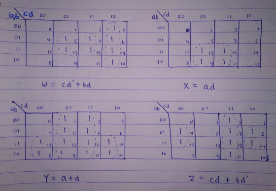
(b.) Using k-map the minimized expression is derived as follows:-
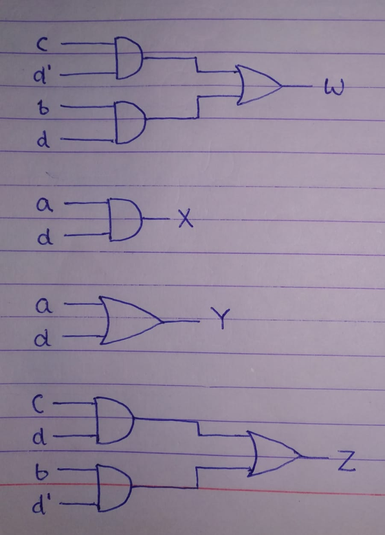
(c.) The implementation of the circuit using logic gates are as follows:-
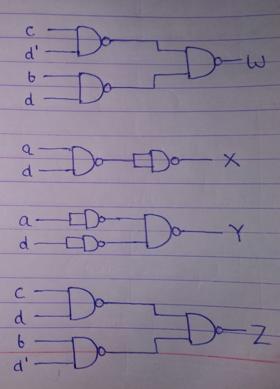
(d.) The implementation of the circuit using NAND gates are as follows:-
Add Answer to:
Click Submit to complete this assessment Questions 10 points Design a digital circuit that reorders the...
DESIGN SECTION Before the experiment, you are going to design a circuit which has 4 inputs...
DESIGN SECTION Before the experiment, you are going to design a circuit which has 4 inputs w, x, y, z and an output F. If 4-bits input value is “odd number which is higher than 4”, or “3-bits highest even number” or “4-bits highest even number”, the output function F will be equal to 1. Otherwise F=0. Each students have to design the circuit and have to do following steps own by own. You are going to; a) Fill the...
Problem 4 Design the static complementary CMOS implementation of a 2-bit comparator circuit, wher...
 Problem 4 Design the static complementary CMOS implementation of a 2-bit comparator circuit, where we have two inputs A and B (each is 2-bit wide) and the output 0 if A > B and output 1 if A B. Design the circuit for minimum delay (assuming a stage effort of 4) and driving a load of 10 fF. As part of the design you need to determine the width of all transistors You can use the following transistor parameters for...
Please show step by step, complete solution and explain if possible. Thank you so much. 3....
 Please show step by step, complete solution and explain if
possible. Thank you so much.
3. Six-Sided Die Display Circuit In this problem, you will design a logic circuit to display the six faces of a die using 7 LEDs. For example, the value 5 is shown on the display below. Your circuit takes three bits XYZ as input and outputs the patterns shown in the table below, by lighting up the correspondind LEDs. For example, for the value 5,...
Please show step by step, complete solution and explain if
possible. Thank you so much.
3. Six-Sided Die Display Circuit In this problem, you will design a logic circuit to display the six faces of a die using 7 LEDs. For example, the value 5 is shown on the display below. Your circuit takes three bits XYZ as input and outputs the patterns shown in the table below, by lighting up the correspondind LEDs. For example, for the value 5,...
**ONLY C&D PLEASE!** (100 points) You are asked to design a "HELLO" circuit in this question....
 **ONLY C&D PLEASE!**
(100 points) You are asked to design a "HELLO" circuit in this question. The inputs of the circuit are three bits x, y and z. The outputs are seven bits a, b, c, d, e, f and g controlling a 7-segment display (see Fig. 2.63(a)). For the 7-segment display, a segment is turned on when the corresponding control signal is 1. The "HELLO" circuit outputs the control signals to display the letter "H", "E", "L", "L", "O"...
**ONLY C&D PLEASE!**
(100 points) You are asked to design a "HELLO" circuit in this question. The inputs of the circuit are three bits x, y and z. The outputs are seven bits a, b, c, d, e, f and g controlling a 7-segment display (see Fig. 2.63(a)). For the 7-segment display, a segment is turned on when the corresponding control signal is 1. The "HELLO" circuit outputs the control signals to display the letter "H", "E", "L", "L", "O"...
Digital Logic Fundamentals. Need help with this assignment!!! Want to make sure I'm on the right ...
 Digital Logic Fundamentals. Need help with this
assignment!!!
Want to make sure I'm on the right track with the truth table
and K-MAPS.
Also I'd like to know how to design the LOGISIM circuit.
Thank you.
igital Logic Fundamentals An Excess-3 code exists for the following reason: The primary advantage of excess-3 coding over non-biased coding is that a decimal number can be nines' complemented (for subtraction) as easily as a binary number can be ones' complemented: just by inverting...
Digital Logic Fundamentals. Need help with this
assignment!!!
Want to make sure I'm on the right track with the truth table
and K-MAPS.
Also I'd like to know how to design the LOGISIM circuit.
Thank you.
igital Logic Fundamentals An Excess-3 code exists for the following reason: The primary advantage of excess-3 coding over non-biased coding is that a decimal number can be nines' complemented (for subtraction) as easily as a binary number can be ones' complemented: just by inverting...
NYIT. Digital Logic Fundamentals, Dr. S. Ben-Avi. Spring 2019. An Excess-3 code exists for the fo...
 I
NEED THE LOGISIM CIRCUIT DESIGN!
NYIT. Digital Logic Fundamentals, Dr. S. Ben-Avi. Spring 2019. An Excess-3 code exists for the following reason: The primary advantage of excess-3 coding over non-biased co ding is that a decimal number can be nines' complemented (for subtraction) as easily as a binary number can be ones' complemented: just by inverting all bits it's useful We shall be discussing complement systems again later in the course - just know that this o Design logic...
I
NEED THE LOGISIM CIRCUIT DESIGN!
NYIT. Digital Logic Fundamentals, Dr. S. Ben-Avi. Spring 2019. An Excess-3 code exists for the following reason: The primary advantage of excess-3 coding over non-biased co ding is that a decimal number can be nines' complemented (for subtraction) as easily as a binary number can be ones' complemented: just by inverting all bits it's useful We shall be discussing complement systems again later in the course - just know that this o Design logic...
1&2 and please I need quickly. Q1 (35 pts): Design a combinational circuit that takes 8...
 1&2 and please I need quickly.
Q1 (35 pts): Design a combinational circuit that takes 8 bits of input and checks iif the inputs are symmetric or not and produces an output immediately. Example: 10011001 or 11000011 produce 1 and 11011010 or 11001100 produce 0.) (a) Write Verilog RTL for this circuit. (b) Same functionality but output appears next cycle. You can instantiate the design in part a. (c) Same functionality but output appeurs after two cycles. You can instantiate...
1&2 and please I need quickly.
Q1 (35 pts): Design a combinational circuit that takes 8 bits of input and checks iif the inputs are symmetric or not and produces an output immediately. Example: 10011001 or 11000011 produce 1 and 11011010 or 11001100 produce 0.) (a) Write Verilog RTL for this circuit. (b) Same functionality but output appears next cycle. You can instantiate the design in part a. (c) Same functionality but output appeurs after two cycles. You can instantiate...
3.4.1 Build and simulate the comparator circuit shown in Figure 3, in Multisim. The inputs A3,...
 3.4.1 Build and simulate the comparator circuit shown in Figure 3, in Multisim. The inputs A3, A2, A1, 40 act as the first 4-bit binary number, and B3, B2, B1, BO act as the second 4-bit binary number. Run your circuit for different setting of the inputs as in Table 3 and observe how the output Xchecks if the numbers are equal or not. Note: connect the eight inputs of this circuit to an 8-input DIP switch as shown in...
Can someone please show me a circuit diagram so i can see how to construct this...
 Can someone please show me a circuit diagram so i can see how to
construct this on a bread board i am id 6 yhanks in advance
EEET-2251: Course & Projoct Guide 2018 EEET-2251: Cousc &Projoct Guide 2018 affic Light Controller A single switch must set your HC74 based state machine to the initial state (the U state This lab will get you to design a simple controller for a pedestrian crossing based on synchronous digital logic. You will master...
Can someone please show me a circuit diagram so i can see how to
construct this on a bread board i am id 6 yhanks in advance
EEET-2251: Course & Projoct Guide 2018 EEET-2251: Cousc &Projoct Guide 2018 affic Light Controller A single switch must set your HC74 based state machine to the initial state (the U state This lab will get you to design a simple controller for a pedestrian crossing based on synchronous digital logic. You will master...
 Problem 4 Design the static complementary CMOS implementation of a 2-bit comparator circuit, where we have two inputs A and B (each is 2-bit wide) and the output 0 if A > B and output 1 if A B. Design the circuit for minimum delay (assuming a stage effort of 4) and driving a load of 10 fF. As part of the design you need to determine the width of all transistors You can use the following transistor parameters for...
 Please show step by step, complete solution and explain if
possible. Thank you so much.
3. Six-Sided Die Display Circuit In this problem, you will design a logic circuit to display the six faces of a die using 7 LEDs. For example, the value 5 is shown on the display below. Your circuit takes three bits XYZ as input and outputs the patterns shown in the table below, by lighting up the correspondind LEDs. For example, for the value 5,...
Please show step by step, complete solution and explain if
possible. Thank you so much.
3. Six-Sided Die Display Circuit In this problem, you will design a logic circuit to display the six faces of a die using 7 LEDs. For example, the value 5 is shown on the display below. Your circuit takes three bits XYZ as input and outputs the patterns shown in the table below, by lighting up the correspondind LEDs. For example, for the value 5,...
 **ONLY C&D PLEASE!**
(100 points) You are asked to design a "HELLO" circuit in this question. The inputs of the circuit are three bits x, y and z. The outputs are seven bits a, b, c, d, e, f and g controlling a 7-segment display (see Fig. 2.63(a)). For the 7-segment display, a segment is turned on when the corresponding control signal is 1. The "HELLO" circuit outputs the control signals to display the letter "H", "E", "L", "L", "O"...
**ONLY C&D PLEASE!**
(100 points) You are asked to design a "HELLO" circuit in this question. The inputs of the circuit are three bits x, y and z. The outputs are seven bits a, b, c, d, e, f and g controlling a 7-segment display (see Fig. 2.63(a)). For the 7-segment display, a segment is turned on when the corresponding control signal is 1. The "HELLO" circuit outputs the control signals to display the letter "H", "E", "L", "L", "O"...
 Digital Logic Fundamentals. Need help with this
assignment!!!
Want to make sure I'm on the right track with the truth table
and K-MAPS.
Also I'd like to know how to design the LOGISIM circuit.
Thank you.
igital Logic Fundamentals An Excess-3 code exists for the following reason: The primary advantage of excess-3 coding over non-biased coding is that a decimal number can be nines' complemented (for subtraction) as easily as a binary number can be ones' complemented: just by inverting...
Digital Logic Fundamentals. Need help with this
assignment!!!
Want to make sure I'm on the right track with the truth table
and K-MAPS.
Also I'd like to know how to design the LOGISIM circuit.
Thank you.
igital Logic Fundamentals An Excess-3 code exists for the following reason: The primary advantage of excess-3 coding over non-biased coding is that a decimal number can be nines' complemented (for subtraction) as easily as a binary number can be ones' complemented: just by inverting...
 I
NEED THE LOGISIM CIRCUIT DESIGN!
NYIT. Digital Logic Fundamentals, Dr. S. Ben-Avi. Spring 2019. An Excess-3 code exists for the following reason: The primary advantage of excess-3 coding over non-biased co ding is that a decimal number can be nines' complemented (for subtraction) as easily as a binary number can be ones' complemented: just by inverting all bits it's useful We shall be discussing complement systems again later in the course - just know that this o Design logic...
I
NEED THE LOGISIM CIRCUIT DESIGN!
NYIT. Digital Logic Fundamentals, Dr. S. Ben-Avi. Spring 2019. An Excess-3 code exists for the following reason: The primary advantage of excess-3 coding over non-biased co ding is that a decimal number can be nines' complemented (for subtraction) as easily as a binary number can be ones' complemented: just by inverting all bits it's useful We shall be discussing complement systems again later in the course - just know that this o Design logic...
 1&2 and please I need quickly.
Q1 (35 pts): Design a combinational circuit that takes 8 bits of input and checks iif the inputs are symmetric or not and produces an output immediately. Example: 10011001 or 11000011 produce 1 and 11011010 or 11001100 produce 0.) (a) Write Verilog RTL for this circuit. (b) Same functionality but output appears next cycle. You can instantiate the design in part a. (c) Same functionality but output appeurs after two cycles. You can instantiate...
1&2 and please I need quickly.
Q1 (35 pts): Design a combinational circuit that takes 8 bits of input and checks iif the inputs are symmetric or not and produces an output immediately. Example: 10011001 or 11000011 produce 1 and 11011010 or 11001100 produce 0.) (a) Write Verilog RTL for this circuit. (b) Same functionality but output appears next cycle. You can instantiate the design in part a. (c) Same functionality but output appeurs after two cycles. You can instantiate...
 3.4.1 Build and simulate the comparator circuit shown in Figure 3, in Multisim. The inputs A3, A2, A1, 40 act as the first 4-bit binary number, and B3, B2, B1, BO act as the second 4-bit binary number. Run your circuit for different setting of the inputs as in Table 3 and observe how the output Xchecks if the numbers are equal or not. Note: connect the eight inputs of this circuit to an 8-input DIP switch as shown in...
 Can someone please show me a circuit diagram so i can see how to
construct this on a bread board i am id 6 yhanks in advance
EEET-2251: Course & Projoct Guide 2018 EEET-2251: Cousc &Projoct Guide 2018 affic Light Controller A single switch must set your HC74 based state machine to the initial state (the U state This lab will get you to design a simple controller for a pedestrian crossing based on synchronous digital logic. You will master...
Can someone please show me a circuit diagram so i can see how to
construct this on a bread board i am id 6 yhanks in advance
EEET-2251: Course & Projoct Guide 2018 EEET-2251: Cousc &Projoct Guide 2018 affic Light Controller A single switch must set your HC74 based state machine to the initial state (the U state This lab will get you to design a simple controller for a pedestrian crossing based on synchronous digital logic. You will master...
Most questions answered within 3 hours.
-
Consider the reaction, C3 H8 + O2 --> CO2 + H2O. How many
moles of O2...
asked 1 hour ago -
You and your opponent both roll a fair die. If you both roll the
same number,...
asked 1 hour ago -
In a study of the accuracy of fast food drive-through orders,
Restaurant A had 257 accurate...
asked 1 hour ago -
Identify and describe in detail the four categories of
institutions that could be included in a...
asked 1 hour ago -
In python
class Customer:
def __init__(self, customer_id, last_name, first_name, phone_number, address):
self._customer_id = int(customer_id)
self._last_name =...
asked 1 hour ago -
What is an example of a limitation in implementing a new
ERP system and how it...
asked 1 hour ago -
In a section of 9.7cm of an artery with a radius of 2.6mm there
is a...
asked 1 hour ago -
the two carboxylic acid groups of aspartic acid have different
acidities with pKa values of 2.1...
asked 1 hour ago -
Would CuCO3 aqueous salt combined with calcium chloride
form a solid precipitate? If so, what would...
asked 1 hour ago -
How do ECM Solutions assist in embedding a culture of continuous
improvement in an organization? (Project...
asked 2 hours ago -
Directions
These directions introduce the idea of Essential Questions.
Since this may be a new concept...
asked 2 hours ago -
1.b. Fiscal policy is said to suffer from ‘crowding out’.
Explain what this means and why...
asked 2 hours ago