The MOS transistor that functions most like a doorbell is what?
The MOS transistor that functions most like a doorbell is
what?
Homework Answers
Answer:-
The most basic element in the design of a large scale integrated
circuit is the transistor. For the processes we will discuss, the
type of transistor available is the Metal-Oxide-Semiconductor Field
Effect Transistor (MOSFET). These transistors are formed as a
``sandwich'' consisting of a semiconductor layer, usually a slice,
or wafer, from a single crystal of silicon; a layer of silicon
dioxide (the oxide) and a layer of metal. These layers are
patterned in a manner which permits transistors to be formed in the
semiconductor material (the ``substrate''); a diagram showing a
typical (idealized) MOSFET is shown in Figure  . Silicon
dioxide is a very good insulator, so a very thin layer, typically
only a few hundred molecules thick, is required. Actually, the
transistors which we will use do not use metal for their gate
regions, but instead use polycrystalline silicon (poly).
Polysilicon gate FET's have replaced virtually all of the older
devices using metal gates in large scale integrated circuits. (Both
metal and polysilicon FET's are sometimes referred to as IGFET's
--- insulated gate field effect transistors, since the silicon
dioxide under the gate is an insulator. We will still continue to
use the term MOSFET to refer to polysilicon gate FET's.)
. Silicon
dioxide is a very good insulator, so a very thin layer, typically
only a few hundred molecules thick, is required. Actually, the
transistors which we will use do not use metal for their gate
regions, but instead use polycrystalline silicon (poly).
Polysilicon gate FET's have replaced virtually all of the older
devices using metal gates in large scale integrated circuits. (Both
metal and polysilicon FET's are sometimes referred to as IGFET's
--- insulated gate field effect transistors, since the silicon
dioxide under the gate is an insulator. We will still continue to
use the term MOSFET to refer to polysilicon gate FET's.)
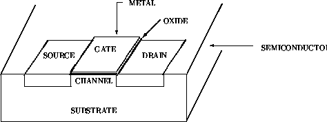
Figure:
The transistor consists of three regions, labeled the
``source'', the ``gate'' and the ``drain''. The area labeled as the
gate region is actually a ``sandwich'' consisting of the underlying
substrate material, which is a single crystal of semiconductor
material (usually silicon); a thin insulating layer (usually
silicon dioxide); and an upper metal layer. Electrical charge, or
current, can flow from the source to the drain depending on the
charge applied to the gate region. The semiconductor material in
the source and drain region are ``doped'' with a different type of
material than in the region under the gate, so an NPN or PNP type
structure exists between the source and drain region of a MOSFET.
Figure shows a
cross section of both types of MOSFET. In Figure (a),
the source and drain regions are doped with N type material and the
substrate doped with P type material. Such a transistor is called
an N channel MOSFET. If they were doped with P type material, and
the substrate doped with N type material as in Figure (b), the
device would be called a P channel MOSFET.

Figure:
The source and drain regions are quite similar, and are labeled depending on to what they are connected. The source is the terminal, or node, which acts as the source of charge carriers; charge carriers leave the source and travel to the drain. In the case of an N channel MOSFET, the source is the more negative of the terminals; in the case of a P channel device, it is the more positive of the terminals. The area under the gate oxide is called the ``channel''.
The MOSFET can operate as a very efficient switch for current
flowing between the source and drain region of the device. For the
simplest type of MOSFET, the ``enhancement mode MOSFET'', which
acts as a ``normally open'' switch, the operation of the device can
be described qualitatively with reference to Figure .

Figure:
Figure (a) shows
an N-channel MOSFET with the source and drain connected to power
( ) and ground
(
) and ground
( ); the
substrate, or body of the device, is also connected to ground. In
this case, there is a reverse biased PN junction between at least
one of the N wells and the substrate, so no current can flow
through the substrate. In particular, there will be no current flow
in the channel region under the gate of the transistor, and
therefore no current will flow between the source and drain of the
device. Under these conditions, the MOSFET is turned
off.
); the
substrate, or body of the device, is also connected to ground. In
this case, there is a reverse biased PN junction between at least
one of the N wells and the substrate, so no current can flow
through the substrate. In particular, there will be no current flow
in the channel region under the gate of the transistor, and
therefore no current will flow between the source and drain of the
device. Under these conditions, the MOSFET is turned
off.
Figure (b) shows
the same N-channel MOSFET with a positive charge applied to the
gate of the device. Under these circumstances, if the gate is given
a sufficiently large charge, negative charge carriers (electrons)
will be attracted from the bulk of the substrate material into the
channel region immediately below the oxide under the gate. When
more electrons are attracted into this region than there are
positive charge carriers (holes) in the channel, then the channel
effectively behaves as an N type region, and current can flow
between the source and the drain. When this happens, the MOSFET is
turned on. Note that a certain minimum charge must be
applied to the gate to overcome the excess of holes already in the
channel region because of the P type doping in the substrate. This
means that the switch is not turned on immediately, rather there
must be some minimum amount of charge applied to the gate before
the transistor is switched on. The voltage which must be applied to
the gate before the transistor allows current to flow between the
source and drain is called the ``threshold voltage'', designated as
 .
.
This type of transistor is called an N channel enhancement mode
MOSFET. (It is called N channel because the conduction in the
channel is due to N type charge carriers; it is said to be an
``enhancement mode'' device because the channel conduction is
enhanced by a charge applied to the gate.) Figure
shows a set of typical characteristic curves for the
current
for the
current  between the
drain and source of a MOSFET as a function of the voltage
between the
drain and source of a MOSFET as a function of the voltage  for a
range of gate voltages,
for a
range of gate voltages,  .
.
Mos transistor Given a combinational logic circuit as shown in Figure Q3 Output NOT Gates A...
 Mos transistor
Given a combinational logic circuit as shown in Figure Q3 Output NOT Gates A Output AND Gates D B Output NOT Gates Figure 03 Determine how many transistor is needed to build it and sketch the transistor connectivity to form the circuit [10 marks)
Mos transistor
Given a combinational logic circuit as shown in Figure Q3 Output NOT Gates A Output AND Gates D B Output NOT Gates Figure 03 Determine how many transistor is needed to build it and sketch the transistor connectivity to form the circuit [10 marks)
Q2. a) Draw the cross-sectional view of ann channel MOS transistor. Label the necessary parts (L,...
 Q2. a) Draw the cross-sectional view of ann channel MOS transistor. Label the necessary parts (L, W, toi, D,G,S, etc.) Give appropriate values for L, W, tox. (10 p) b) Explain, how an n-channel enhancement mode MOS transistor operates. (10p)
6. Consider an N MOS transistor with μ nCa.-100μA/V", Vi = 0.5V, WL = 10, was...
 6. Consider an N MOS transistor with μ nCa.-100μA/V", Vi = 0.5V, WL = 10, was = 5V and vis-IV a. What is the estimated drain current? (10%) b, when VGs = 5V and vos = 5V, what is the estimated drain current? (1096)
14. are available only 7 n- Implement the functions A+B, C+A.D and A+B+C (there MOS and...
 14. are available only 7 n- Implement the functions A+B, C+A.D and A+B+C (there MOS and 7 p-MOS transistors for all functions combined, only A, B and C are available as inputs) 15. Implement the function A+B.(C-D+E) in typical CMOS (there are available only 5 n- MOS and 5 p-MOS transistors, only A, B, C, D and E are available as inputs)
Problem 1. An n-channel MOS transistor is fabricated with the following specifications: Substrate is a p-type...
Problem 1. An n-channel MOS transistor is fabricated with the following specifications: Substrate is a p-type silicon with doping concentration NA=2x1015 cm-3 . The SiO2 gate thickness is 200 Å. Effective interface charges Qi=6.5x10⁻⁹ col/cm2. Work function difference between gate conductor and silicon substrate qфms=-0.95 eV. Calculate the following: a. Maximum depletion width, with respect to ground b. Gate capacitance per unit area, Ci c. Flat-band voltage, VFB d. Threshold voltage, VT.
What is the most ely pruct of the follon ing d Whar is the mos e...
 What is the most ely pruct of the follon ing d Whar is the mos e pract ofthe ollowing reaction? DIBAH-78 HO Question #6 1 10 points! Which of the following reagents will best complete the reaction below? 1. L?AIH. NaRH, Na LIAHO4u)-7C 1.DIBAH-78 1.NaH 2. H 2.H,0 IV b. Circle the less reactive functional group in the above molecule c. What is the most likely product of the following reaction? NaBll (excess) McOlI
It is possible to use the bulk terminal of a transistor as an input of an...
 It is possible to use the bulk terminal of a transistor as an
input of an amplifier. Consider the single-stage NMOS amplifier
shown below.
For Vbias=1.5V: a) What is the region of operation of the transistor? b) Calculate the small-signal gain (A =V2/Vin) of the amplifier. Recall that gmbr ngm- Assume, 1 = 0, n=0.2, VTHONMOS= 0.5V, uCox=100 A/V2, Rp=1k2, (W/L)Mos= 20, and VDD=3V.
It is possible to use the bulk terminal of a transistor as an
input of an amplifier. Consider the single-stage NMOS amplifier
shown below.
For Vbias=1.5V: a) What is the region of operation of the transistor? b) Calculate the small-signal gain (A =V2/Vin) of the amplifier. Recall that gmbr ngm- Assume, 1 = 0, n=0.2, VTHONMOS= 0.5V, uCox=100 A/V2, Rp=1k2, (W/L)Mos= 20, and VDD=3V.
4) (25 points) Suppose your doorbell rings and it is your neighbors son, offering to weed your flowerbed, which goes all the way around your house. You would like to have it weeded but cannot sta...
 4) (25 points) Suppose your doorbell rings and it is your neighbors son, offering to weed your flowerbed, which goes all the way around your house. You would like to have it weeded but cannot stay to supervise. Should you offer to pay by the hour, pay a fized fee, or pay by the weight of the weeds picked? What is the person doing the weeding likely to prefer?
4) (25 points) Suppose your doorbell rings and it is your...
4) (25 points) Suppose your doorbell rings and it is your neighbors son, offering to weed your flowerbed, which goes all the way around your house. You would like to have it weeded but cannot stay to supervise. Should you offer to pay by the hour, pay a fized fee, or pay by the weight of the weeds picked? What is the person doing the weeding likely to prefer?
4) (25 points) Suppose your doorbell rings and it is your...
Sketch structure of depletion-enhancement MOS Filed Effect Transistor (DE-MOSFET). Explain essence of principle of operation of E-MOSFET connected in common-source configuration. Sketch and explain sh...
Sketch structure of depletion-enhancement MOS Filed Effect Transistor (DE-MOSFET). Explain essence of principle of operation of E-MOSFET connected in common-source configuration. Sketch and explain shapes of corresponding common-source transfer curves and common-source output curves (drain IV characteristics). Explain why input IV characteristics are not used in the case of FET.
DBMS has many functions. What three functions are the most important and why are they most...
DBMS has many functions. What three functions are the most important and why are they most important? What one benefit of a DBMS would you be willing to give up and why?
 Mos transistor
Given a combinational logic circuit as shown in Figure Q3 Output NOT Gates A Output AND Gates D B Output NOT Gates Figure 03 Determine how many transistor is needed to build it and sketch the transistor connectivity to form the circuit [10 marks)
Mos transistor
Given a combinational logic circuit as shown in Figure Q3 Output NOT Gates A Output AND Gates D B Output NOT Gates Figure 03 Determine how many transistor is needed to build it and sketch the transistor connectivity to form the circuit [10 marks)
 Q2. a) Draw the cross-sectional view of ann channel MOS transistor. Label the necessary parts (L, W, toi, D,G,S, etc.) Give appropriate values for L, W, tox. (10 p) b) Explain, how an n-channel enhancement mode MOS transistor operates. (10p)
 6. Consider an N MOS transistor with μ nCa.-100μA/V", Vi = 0.5V, WL = 10, was = 5V and vis-IV a. What is the estimated drain current? (10%) b, when VGs = 5V and vos = 5V, what is the estimated drain current? (1096)
 14. are available only 7 n- Implement the functions A+B, C+A.D and A+B+C (there MOS and 7 p-MOS transistors for all functions combined, only A, B and C are available as inputs) 15. Implement the function A+B.(C-D+E) in typical CMOS (there are available only 5 n- MOS and 5 p-MOS transistors, only A, B, C, D and E are available as inputs)
 What is the most ely pruct of the follon ing d Whar is the mos e pract ofthe ollowing reaction? DIBAH-78 HO Question #6 1 10 points! Which of the following reagents will best complete the reaction below? 1. L?AIH. NaRH, Na LIAHO4u)-7C 1.DIBAH-78 1.NaH 2. H 2.H,0 IV b. Circle the less reactive functional group in the above molecule c. What is the most likely product of the following reaction? NaBll (excess) McOlI
 It is possible to use the bulk terminal of a transistor as an
input of an amplifier. Consider the single-stage NMOS amplifier
shown below.
For Vbias=1.5V: a) What is the region of operation of the transistor? b) Calculate the small-signal gain (A =V2/Vin) of the amplifier. Recall that gmbr ngm- Assume, 1 = 0, n=0.2, VTHONMOS= 0.5V, uCox=100 A/V2, Rp=1k2, (W/L)Mos= 20, and VDD=3V.
It is possible to use the bulk terminal of a transistor as an
input of an amplifier. Consider the single-stage NMOS amplifier
shown below.
For Vbias=1.5V: a) What is the region of operation of the transistor? b) Calculate the small-signal gain (A =V2/Vin) of the amplifier. Recall that gmbr ngm- Assume, 1 = 0, n=0.2, VTHONMOS= 0.5V, uCox=100 A/V2, Rp=1k2, (W/L)Mos= 20, and VDD=3V.
 4) (25 points) Suppose your doorbell rings and it is your neighbors son, offering to weed your flowerbed, which goes all the way around your house. You would like to have it weeded but cannot stay to supervise. Should you offer to pay by the hour, pay a fized fee, or pay by the weight of the weeds picked? What is the person doing the weeding likely to prefer?
4) (25 points) Suppose your doorbell rings and it is your...
4) (25 points) Suppose your doorbell rings and it is your neighbors son, offering to weed your flowerbed, which goes all the way around your house. You would like to have it weeded but cannot stay to supervise. Should you offer to pay by the hour, pay a fized fee, or pay by the weight of the weeds picked? What is the person doing the weeding likely to prefer?
4) (25 points) Suppose your doorbell rings and it is your...
Most questions answered within 3 hours.
-
Argue for or against the "Three Strikes"laws. Provide a rationale
to support your response.
asked 29 minutes ago -
Bargaining Models: what is the "Obsolescing Bargain"?
Bargaining Models: what are the factors that would tend...
asked 1 hour ago -
1. A ball is thrown up into the air.
a) Draw motion diagram and the point-like...
asked 1 hour ago -
1) Because money eliminates the "double coincidence of wants"
problem, the development of money as a...
asked 2 hours ago -
Company AAA produces only one product which other manufacturers
purchase as a component for their final...
asked 4 hours ago -
An
item can be appended to an array-based list, provided the lenght is
less than the...
asked 4 hours ago -
Two particles each have a rest mass energy of 30 MeV and are
traveling with a...
asked 6 hours ago -
why
is vectorization a faster alternative to loops?
asked 7 hours ago -
General Matter’s outstanding bond issue has a coupon rate of
11.8%, and it sells at a...
asked 7 hours ago -
Write a one page essay on how important is it to know your basic
accounting knowledge...
asked 7 hours ago -
You are a Senior Civil Engineer posted at the Contracts and
Procurement Division of the Ministry...
asked 7 hours ago -
When using the percentage of completion method, the
company
- recognizes revenues and gross profit each...
asked 7 hours ago