
Homework Answers

Add Answer to:
Problem 6: The energy band diagram for an ideal MOS-capacitor is shown below. tx 0.2 μm and Ep = E, at the Si-SiO2 interface. Assume no oxide charge and φ'm5-0. Answer the following. EpM Eps T...
Need help with i) please! 2. The energy band diagram for an ideal xo-0.2um MOS-C operated...
 Need help with i) please!
2. The energy band diagram for an ideal xo-0.2um MOS-C operated at T-300K is sketched in Figure 1. Note that the applied gate voltage causes band bending in the semiconductor such that Ef Ei at the Si-SiO2 interface. a) Sketch the electrostatic potential () inside the semiconductor as a function of position b) Roughly sketch the electric field (5) inside the oxide and semiconductor as a function of position. c) Do equilibrium conditions prevail inside...
Need help with i) please!
2. The energy band diagram for an ideal xo-0.2um MOS-C operated at T-300K is sketched in Figure 1. Note that the applied gate voltage causes band bending in the semiconductor such that Ef Ei at the Si-SiO2 interface. a) Sketch the electrostatic potential () inside the semiconductor as a function of position b) Roughly sketch the electric field (5) inside the oxide and semiconductor as a function of position. c) Do equilibrium conditions prevail inside...
Subject : Semiconductor topic MOS + 1. Figure 1 illustrates the energy band diagram of a...
 Subject :
Semiconductor
topic MOS
+ 1. Figure 1 illustrates the energy band diagram of a Metal-Oxide-Semiconductor (MOS). Based on the Figure 1 and the given parameters, Semicon surface Ec Figure 1 a) write the posson's equation that relates the potential and distance from the oxide-semiconductor interface b) write the mathematical relationship of the surface potential as a function of substrate doping concentration when the surface is under strong inversion condition c) write the equation for the maximum width of...
Subject :
Semiconductor
topic MOS
+ 1. Figure 1 illustrates the energy band diagram of a Metal-Oxide-Semiconductor (MOS). Based on the Figure 1 and the given parameters, Semicon surface Ec Figure 1 a) write the posson's equation that relates the potential and distance from the oxide-semiconductor interface b) write the mathematical relationship of the surface potential as a function of substrate doping concentration when the surface is under strong inversion condition c) write the equation for the maximum width of...
Problem 5: The gate capacitance vs. gate voltage characteristic of a p+ poly-Si gated MOS capacitor of area 1x10"cm', is as shown: Assume Esi = 11.9, Eox-39,E,-8.85 × 10⁻¹⁴ F/on, and nl =...
 Problem 5: The gate capacitance vs. gate voltage characteristic of a p+ poly-Si gated MOS capacitor of area 1x10"cm', is as shown: Assume Esi = 11.9, Eox-39,E,-8.85 × 10⁻¹⁴ F/on, and nl = 1.5 x 1010 cm3 Co [Farads] 3.45x10¹¹ >Va [Volts] 1.0 0.3 (a) Is the semiconductor (silicon) substrate doped n-type or p-type? Explain briefly. (b) Is the measurement frequency low or high? Explain briefly. (c) What is the thickness of the gate oxide (SiO2), xo? (d) Estimate the...
Problem3: Consider a MOS capacitor maintained at T 300K with the following characteristics: Assume Esi 1.9,x 3.9,8.85 x 10-14 F/cm, and n 1.5 x 1010cm3 . Gate material is n+ poly-silicon . Total n...
 Problem3: Consider a MOS capacitor maintained at T 300K with the following characteristics: Assume Esi 1.9,x 3.9,8.85 x 10-14 F/cm, and n 1.5 x 1010cm3 . Gate material is n+ poly-silicon . Total negative oxide charge of 5x 10¹¹q C/cnm2 . Substrate is n-type Si, with doping concentration 1x1016 cm3 Oxide thickness 5 nm . The electron affinity for Si is 4.03eV? a) Draw the band diagram at equilibrium. b) From part (a). What is the substrate (bulk) condition at...
Problem 3: Consider a MOS capacitor maintained at T= 300K with the following characteristics: Assume s 11.9, ox 3.9, 8.85x 10⁻¹ F/cm, and n 1.5 x 1010cm3 Gate material is n poly-silicon Total...
 Problem 3: Consider a MOS capacitor maintained at T= 300K with the following characteristics: Assume s 11.9, ox 3.9, 8.85x 10⁻¹ F/cm, and n 1.5 x 1010cm3 Gate material is n poly-silicon Total negative oxide charge of 5x 10¹¹q C/cm . Substrate is n-type Si, with doping concentration 1 x1016 cm-3 Oxide thickness 5 nmm The electron affinity for Si is 4.03eV? e) What is the flat capacitance? f) What is the depletion region width? g) What is the potential...
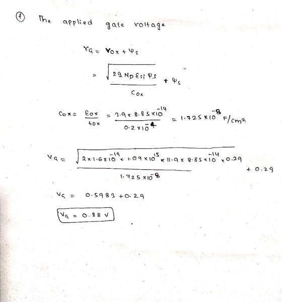
(15 pts) 14. The energy band diagram for an ideal MOS-C under a specific gate bias is shown below...
 Please do d e and f
(15 pts) 14. The energy band diagram for an ideal MOS-C under a specific gate bias is shown below. The device is maintained at T 300 K, kTiq 0.026 V, n, 1010 cm Note that E EF at the surface of the semiconductor. Answer the following questions. (d) Determine the surface potential s. (3 pts) EFM 0.24eVEc (e) Determine Dr. (3 pts) E, 0437 ev Ev 0 (a) What biasing mode is this MOS-C...
Please do d e and f
(15 pts) 14. The energy band diagram for an ideal MOS-C under a specific gate bias is shown below. The device is maintained at T 300 K, kTiq 0.026 V, n, 1010 cm Note that E EF at the surface of the semiconductor. Answer the following questions. (d) Determine the surface potential s. (3 pts) EFM 0.24eVEc (e) Determine Dr. (3 pts) E, 0437 ev Ev 0 (a) What biasing mode is this MOS-C...
Problem l: The capacitance vs. gate voltage characteristic of a simple MOS capacitor of area 100 μιηχ 1 00pm is as shown: Assume Esi-1 1.9, Eox-3.9, Eo-8.85 >< 10-14 F/cm, and ni-1.5x 1010cm...
 Problem l: The capacitance vs. gate voltage characteristic of a simple MOS capacitor of area 100 μιηχ 1 00pm is as shown: Assume Esi-1 1.9, Eox-3.9, Eo-8.85 >< 10-14 F/cm, and ni-1.5x 1010cm3 C (pF) 70 ECV) 0.25 a) What is the thickness of the gate oxide (Sio2)? b) Does the capacitor have a metal gate or poly-Si gate? Why? c) Is the substrate n-type or p-type? How do you know? d) Estimate the values of VFB and VrH. e)...
 Need help with i) please!
2. The energy band diagram for an ideal xo-0.2um MOS-C operated at T-300K is sketched in Figure 1. Note that the applied gate voltage causes band bending in the semiconductor such that Ef Ei at the Si-SiO2 interface. a) Sketch the electrostatic potential () inside the semiconductor as a function of position b) Roughly sketch the electric field (5) inside the oxide and semiconductor as a function of position. c) Do equilibrium conditions prevail inside...
Need help with i) please!
2. The energy band diagram for an ideal xo-0.2um MOS-C operated at T-300K is sketched in Figure 1. Note that the applied gate voltage causes band bending in the semiconductor such that Ef Ei at the Si-SiO2 interface. a) Sketch the electrostatic potential () inside the semiconductor as a function of position b) Roughly sketch the electric field (5) inside the oxide and semiconductor as a function of position. c) Do equilibrium conditions prevail inside...
 Subject :
Semiconductor
topic MOS
+ 1. Figure 1 illustrates the energy band diagram of a Metal-Oxide-Semiconductor (MOS). Based on the Figure 1 and the given parameters, Semicon surface Ec Figure 1 a) write the posson's equation that relates the potential and distance from the oxide-semiconductor interface b) write the mathematical relationship of the surface potential as a function of substrate doping concentration when the surface is under strong inversion condition c) write the equation for the maximum width of...
Subject :
Semiconductor
topic MOS
+ 1. Figure 1 illustrates the energy band diagram of a Metal-Oxide-Semiconductor (MOS). Based on the Figure 1 and the given parameters, Semicon surface Ec Figure 1 a) write the posson's equation that relates the potential and distance from the oxide-semiconductor interface b) write the mathematical relationship of the surface potential as a function of substrate doping concentration when the surface is under strong inversion condition c) write the equation for the maximum width of...
 Problem 5: The gate capacitance vs. gate voltage characteristic of a p+ poly-Si gated MOS capacitor of area 1x10"cm', is as shown: Assume Esi = 11.9, Eox-39,E,-8.85 × 10⁻¹⁴ F/on, and nl = 1.5 x 1010 cm3 Co [Farads] 3.45x10¹¹ >Va [Volts] 1.0 0.3 (a) Is the semiconductor (silicon) substrate doped n-type or p-type? Explain briefly. (b) Is the measurement frequency low or high? Explain briefly. (c) What is the thickness of the gate oxide (SiO2), xo? (d) Estimate the...
 Problem3: Consider a MOS capacitor maintained at T 300K with the following characteristics: Assume Esi 1.9,x 3.9,8.85 x 10-14 F/cm, and n 1.5 x 1010cm3 . Gate material is n+ poly-silicon . Total negative oxide charge of 5x 10¹¹q C/cnm2 . Substrate is n-type Si, with doping concentration 1x1016 cm3 Oxide thickness 5 nm . The electron affinity for Si is 4.03eV? a) Draw the band diagram at equilibrium. b) From part (a). What is the substrate (bulk) condition at...
 Problem 3: Consider a MOS capacitor maintained at T= 300K with the following characteristics: Assume s 11.9, ox 3.9, 8.85x 10⁻¹ F/cm, and n 1.5 x 1010cm3 Gate material is n poly-silicon Total negative oxide charge of 5x 10¹¹q C/cm . Substrate is n-type Si, with doping concentration 1 x1016 cm-3 Oxide thickness 5 nmm The electron affinity for Si is 4.03eV? e) What is the flat capacitance? f) What is the depletion region width? g) What is the potential...
 Please do d e and f
(15 pts) 14. The energy band diagram for an ideal MOS-C under a specific gate bias is shown below. The device is maintained at T 300 K, kTiq 0.026 V, n, 1010 cm Note that E EF at the surface of the semiconductor. Answer the following questions. (d) Determine the surface potential s. (3 pts) EFM 0.24eVEc (e) Determine Dr. (3 pts) E, 0437 ev Ev 0 (a) What biasing mode is this MOS-C...
Please do d e and f
(15 pts) 14. The energy band diagram for an ideal MOS-C under a specific gate bias is shown below. The device is maintained at T 300 K, kTiq 0.026 V, n, 1010 cm Note that E EF at the surface of the semiconductor. Answer the following questions. (d) Determine the surface potential s. (3 pts) EFM 0.24eVEc (e) Determine Dr. (3 pts) E, 0437 ev Ev 0 (a) What biasing mode is this MOS-C...
 Problem l: The capacitance vs. gate voltage characteristic of a simple MOS capacitor of area 100 μιηχ 1 00pm is as shown: Assume Esi-1 1.9, Eox-3.9, Eo-8.85 >< 10-14 F/cm, and ni-1.5x 1010cm3 C (pF) 70 ECV) 0.25 a) What is the thickness of the gate oxide (Sio2)? b) Does the capacitor have a metal gate or poly-Si gate? Why? c) Is the substrate n-type or p-type? How do you know? d) Estimate the values of VFB and VrH. e)...
Most questions answered within 3 hours.
-
Which of the following pairs of ions have the same electron
configuration?
I: Br− and Se2−...
asked 36 minutes ago -
The Foremost Composite Materials Company is planning a two-day
sales conference for October 19-20. The conference...
asked 58 minutes ago -
3) Illustrate the observed pattern of relatedness of organisms
versus adaptations to specific conditions. This means...
asked 1 hour ago -
In winter a lake has a 0.35 m thick ice layer over 1.10 m of
water....
asked 2 hours ago -
Assuming the following has been encrypted with a Vigenere cipher
below, use the method(s) and assumptions...
asked 2 hours ago -
How would I use switch statements to write a program that will
take an input of...
asked 2 hours ago -
Imagine a reaction in which methane gas combusts at a constant
pressure of 1 atm and...
asked 2 hours ago -
Two parallel wires (each 12 m in length) are separated by a
distance of 0.065 m...
asked 2 hours ago -
Suppose there were three masses at the corner of uniform
equilateral triangle. The masses are m1...
asked 2 hours ago -
Situation: A building that is 618 m above the ground floor. How
many times would a...
asked 2 hours ago -
help me and discuss one successful and one
unsuccessful international company/busines in Indonesia.whyit
succeed and why...
asked 2 hours ago -
I- Choose the best answer
Which of the following statements about the structure and
packaging of...
asked 2 hours ago