P.s last part with explanation be written explicitly if possible. Thx from now on

Homework Answers


Add Answer to:
P.s last part with explanation be written explicitly if
possible. Thx from now on
The question...
Procedure Using the test board, one 7476 Dual JK Flip-Flop chip and a function generator, connect...
 Procedure Using the test board, one 7476 Dual JK Flip-Flop chip and a function generator, connect the circuit shown in Fig-2. The inputs S, R, J and K must be connected to switches, while input C is connected to the function generator to implement the various cases of the inputs. Adjust the function generator to output a 2.5V-peak square wave with a DC offset 2.5V and a 100Hz frequency. Connect the outputs to LEDs. Connect the circuit to the power...
23. A J-K flip-flop has a l on the J input and a 0 on the...
 23. A J-K flip-flop has a l on the J input and a 0 on the K input. What state is the flip-flop in? (a) Q=1,0-0 (b) Q-1, Q-1 (c) Q-0,Q 1 (d) Q-0,Q-0 -24. On a positive edge-triggered S-R flip-flop, the outputs reflect the input condition when (a) the clock pulse is LOW (b) the clock pulse is HIGH (c) the clock pulse transitions from LOW to HIGH (d) the clock pulse transitions from HIGH to LOW 25. The...
QUESTION 7 A master slave flip flop behaves similarly to a clocked latch, except that the...
 QUESTION 7 A master slave flip flop behaves similarly to a clocked latch, except that the latches output can change only near the rising edge of the clock True False QUESTION 8 Assuming zero setup and hold times, clocked latches and flip-flops produce the same outputs as long as the inputs do not change while the clock is asserted True False QUESTIONS An edge-triggered D flip-flop requires more internal gates than a similar device constructed from a J-K master-slave flip...
how slove 4-34, 4-35, 4-36??? I dont know that! please hlep me! 306 □ CHAPTER 4/SEQUENTIAL CIRCUITS OTABLE 4-16...
 how slove 4-34, 4-35, 4-36??? I dont know that! please hlep me!
306 □ CHAPTER 4/SEQUENTIAL CIRCUITS OTABLE 4-16 State Table for Problem 4-33 Next State Input Output Present State 4-36 4-37 0 0 0 0 4-38 Design the circuit specified by Table 4-14 and use the sequence from Problen 4-31 (either yours or the one posted on the text website) to perform an automatic logic simulation-based verification of your design. 4 433. The state table for a sequential circuit...
how slove 4-34, 4-35, 4-36??? I dont know that! please hlep me!
306 □ CHAPTER 4/SEQUENTIAL CIRCUITS OTABLE 4-16 State Table for Problem 4-33 Next State Input Output Present State 4-36 4-37 0 0 0 0 4-38 Design the circuit specified by Table 4-14 and use the sequence from Problen 4-31 (either yours or the one posted on the text website) to perform an automatic logic simulation-based verification of your design. 4 433. The state table for a sequential circuit...
1. Write the Boolean expression for each output from the PLA below: F = F G...
 1. Write the Boolean expression for each output from the PLA below: F = F G H 2. Draw the block diagram (not logic gates) and the truth table for a 4-1 multiplexer. Label all inputs, outputs and select lines. 3. Explain the problem with the S-R latch and how it is fixed by the J-K flip-flop 4. Write the truth table for a Gated D Latch: 5. Complete the following timing diagram for the rising-edge-triggered D flip-flop: akrrrr G1
Need help part B and C please. Thank you . CDA3201·Intro to Logic Desig Lab Assignment...
 Need help part B and C please. Thank you
. CDA3201·Intro to Logic Desig Lab Assignment Name: Grade: 20 5) 120] At right is the state dingram for a Moore sequential 1 01.10 АО circuit which monitors two inputs XiXo. When the two inputs XiXo are 00, the output Z toggles at every clock When the two inputs XiXo are 11, the output Z toggles at every other clock. When the two inputs XiXo are different, the output Z holds...
Need help part B and C please. Thank you
. CDA3201·Intro to Logic Desig Lab Assignment Name: Grade: 20 5) 120] At right is the state dingram for a Moore sequential 1 01.10 АО circuit which monitors two inputs XiXo. When the two inputs XiXo are 00, the output Z toggles at every clock When the two inputs XiXo are 11, the output Z toggles at every other clock. When the two inputs XiXo are different, the output Z holds...
please solve the question completely and show the steps ... thumb up will be given (5 points each) [CO: 6] a. If RO and R1 are both 16-bit serial shift registers, each with a single serial input (S_IN...
 please solve the question completely and show the steps ...
thumb up will be given
(5 points each) [CO: 6] a. If RO and R1 are both 16-bit serial shift registers, each with a single serial input (S_IN) and a single serial output (S_OUT), clock and reset. Design using RO and Rl additional logic, a circuit that would store the output S_OUT of either RO or Rl into a D-FF based on input CH. If CH is 0, S OUT...
please solve the question completely and show the steps ...
thumb up will be given
(5 points each) [CO: 6] a. If RO and R1 are both 16-bit serial shift registers, each with a single serial input (S_IN) and a single serial output (S_OUT), clock and reset. Design using RO and Rl additional logic, a circuit that would store the output S_OUT of either RO or Rl into a D-FF based on input CH. If CH is 0, S OUT...
Q1) If R0 and R1 are both 16-bit serial shift registers, each with a single serial input (S_IN) and a single serial output (S_OUT), clock and reset. Design using R0 and R1 additional logic, a circuit...
Q1) If R0 and R1 are both 16-bit serial shift registers, each with a single serial input (S_IN) and a single serial output (S_OUT), clock and reset. Design using R0 and R1 additional logic, a circuit that would store the output S_OUT of either R0 or R1 into a D-FF based on input CH. If CH is 0, S OUT of R0 will be stored in the D-FF (at the edge of the clock) and if CH is 1, S_OUT...
please, Teacher, help me with this question step by step please and explain everything, my Teacher?...
 please, Teacher, help me with this question step by step please
and explain everything, my Teacher?
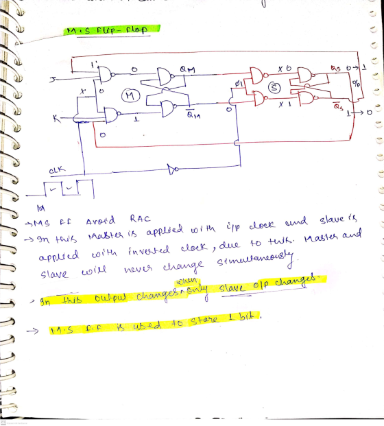
EENG 250 Lab 4 M&N Flip Flop Intorduction: There are four types of latches or flip flop designs that are commonly used in designs. However it is always possible to create a custom design. For example take the JK Flip Flop. It can be built using a D Flip Flop. This can be done using state diagram design processes. As shown in the example...
please, Teacher, help me with this question step by step please
and explain everything, my Teacher?
EENG 250 Lab 4 M&N Flip Flop Intorduction: There are four types of latches or flip flop designs that are commonly used in designs. However it is always possible to create a custom design. For example take the JK Flip Flop. It can be built using a D Flip Flop. This can be done using state diagram design processes. As shown in the example...
please help question 2 2. Design a half-adder with the constraint that you can only use...
 please help question 2
2. Design a half-adder with the constraint that you can only use NAND and NOR gates. The circuit inputs are two bits I and y and the outputs are the sum bit s and carry bit c. Draw a circuit diagram and label each input and output. 3. The digital circuit below contains a latch and two flip-flops. Use the wave forms provided to find Qa. Qb, and Qe. Assume that all three states have initial...
please help question 2
2. Design a half-adder with the constraint that you can only use NAND and NOR gates. The circuit inputs are two bits I and y and the outputs are the sum bit s and carry bit c. Draw a circuit diagram and label each input and output. 3. The digital circuit below contains a latch and two flip-flops. Use the wave forms provided to find Qa. Qb, and Qe. Assume that all three states have initial...
 Procedure Using the test board, one 7476 Dual JK Flip-Flop chip and a function generator, connect the circuit shown in Fig-2. The inputs S, R, J and K must be connected to switches, while input C is connected to the function generator to implement the various cases of the inputs. Adjust the function generator to output a 2.5V-peak square wave with a DC offset 2.5V and a 100Hz frequency. Connect the outputs to LEDs. Connect the circuit to the power...
 23. A J-K flip-flop has a l on the J input and a 0 on the K input. What state is the flip-flop in? (a) Q=1,0-0 (b) Q-1, Q-1 (c) Q-0,Q 1 (d) Q-0,Q-0 -24. On a positive edge-triggered S-R flip-flop, the outputs reflect the input condition when (a) the clock pulse is LOW (b) the clock pulse is HIGH (c) the clock pulse transitions from LOW to HIGH (d) the clock pulse transitions from HIGH to LOW 25. The...
 QUESTION 7 A master slave flip flop behaves similarly to a clocked latch, except that the latches output can change only near the rising edge of the clock True False QUESTION 8 Assuming zero setup and hold times, clocked latches and flip-flops produce the same outputs as long as the inputs do not change while the clock is asserted True False QUESTIONS An edge-triggered D flip-flop requires more internal gates than a similar device constructed from a J-K master-slave flip...
 how slove 4-34, 4-35, 4-36??? I dont know that! please hlep me!
306 □ CHAPTER 4/SEQUENTIAL CIRCUITS OTABLE 4-16 State Table for Problem 4-33 Next State Input Output Present State 4-36 4-37 0 0 0 0 4-38 Design the circuit specified by Table 4-14 and use the sequence from Problen 4-31 (either yours or the one posted on the text website) to perform an automatic logic simulation-based verification of your design. 4 433. The state table for a sequential circuit...
how slove 4-34, 4-35, 4-36??? I dont know that! please hlep me!
306 □ CHAPTER 4/SEQUENTIAL CIRCUITS OTABLE 4-16 State Table for Problem 4-33 Next State Input Output Present State 4-36 4-37 0 0 0 0 4-38 Design the circuit specified by Table 4-14 and use the sequence from Problen 4-31 (either yours or the one posted on the text website) to perform an automatic logic simulation-based verification of your design. 4 433. The state table for a sequential circuit...
 1. Write the Boolean expression for each output from the PLA below: F = F G H 2. Draw the block diagram (not logic gates) and the truth table for a 4-1 multiplexer. Label all inputs, outputs and select lines. 3. Explain the problem with the S-R latch and how it is fixed by the J-K flip-flop 4. Write the truth table for a Gated D Latch: 5. Complete the following timing diagram for the rising-edge-triggered D flip-flop: akrrrr G1
 Need help part B and C please. Thank you
. CDA3201·Intro to Logic Desig Lab Assignment Name: Grade: 20 5) 120] At right is the state dingram for a Moore sequential 1 01.10 АО circuit which monitors two inputs XiXo. When the two inputs XiXo are 00, the output Z toggles at every clock When the two inputs XiXo are 11, the output Z toggles at every other clock. When the two inputs XiXo are different, the output Z holds...
Need help part B and C please. Thank you
. CDA3201·Intro to Logic Desig Lab Assignment Name: Grade: 20 5) 120] At right is the state dingram for a Moore sequential 1 01.10 АО circuit which monitors two inputs XiXo. When the two inputs XiXo are 00, the output Z toggles at every clock When the two inputs XiXo are 11, the output Z toggles at every other clock. When the two inputs XiXo are different, the output Z holds...
 please solve the question completely and show the steps ...
thumb up will be given
(5 points each) [CO: 6] a. If RO and R1 are both 16-bit serial shift registers, each with a single serial input (S_IN) and a single serial output (S_OUT), clock and reset. Design using RO and Rl additional logic, a circuit that would store the output S_OUT of either RO or Rl into a D-FF based on input CH. If CH is 0, S OUT...
please solve the question completely and show the steps ...
thumb up will be given
(5 points each) [CO: 6] a. If RO and R1 are both 16-bit serial shift registers, each with a single serial input (S_IN) and a single serial output (S_OUT), clock and reset. Design using RO and Rl additional logic, a circuit that would store the output S_OUT of either RO or Rl into a D-FF based on input CH. If CH is 0, S OUT...
 please, Teacher, help me with this question step by step please
and explain everything, my Teacher?
EENG 250 Lab 4 M&N Flip Flop Intorduction: There are four types of latches or flip flop designs that are commonly used in designs. However it is always possible to create a custom design. For example take the JK Flip Flop. It can be built using a D Flip Flop. This can be done using state diagram design processes. As shown in the example...
please, Teacher, help me with this question step by step please
and explain everything, my Teacher?
EENG 250 Lab 4 M&N Flip Flop Intorduction: There are four types of latches or flip flop designs that are commonly used in designs. However it is always possible to create a custom design. For example take the JK Flip Flop. It can be built using a D Flip Flop. This can be done using state diagram design processes. As shown in the example...
 please help question 2
2. Design a half-adder with the constraint that you can only use NAND and NOR gates. The circuit inputs are two bits I and y and the outputs are the sum bit s and carry bit c. Draw a circuit diagram and label each input and output. 3. The digital circuit below contains a latch and two flip-flops. Use the wave forms provided to find Qa. Qb, and Qe. Assume that all three states have initial...
please help question 2
2. Design a half-adder with the constraint that you can only use NAND and NOR gates. The circuit inputs are two bits I and y and the outputs are the sum bit s and carry bit c. Draw a circuit diagram and label each input and output. 3. The digital circuit below contains a latch and two flip-flops. Use the wave forms provided to find Qa. Qb, and Qe. Assume that all three states have initial...
Most questions answered within 3 hours.
-
An entomologist discovers a dung beetle rolling a ball of dung
along the ground, and decides...
asked 14 minutes ago -
Humans have used horses for transportation for millions of
years. Therefore, they will use horses for...
asked 2 hours ago -
The following are the Jensen Corporation's unit costs of making
and selling an item at a...
asked 2 hours ago -
Does direct Medicare reimbursement of Advanced practice nurses
increase access to their services?
asked 3 hours ago -
List and explain why a company would choose to use a
published
compensation survey vs. creating...
asked 3 hours ago -
A discrete random variable X can take values from 1 to 10. Find
the variance of...
asked 3 hours ago -
The primary financial goal of a corporation is to maximize:
shareholders wealth.
earnings per share.
stock...
asked 4 hours ago -
determine whether the vectors u=(1,2,3,), v=(-2,1,0) and
w=(1,0,1) are linearly dependent or independent.
asked 4 hours ago -
python
Define a function called print_values which takes a dictionary
object as a parameter. The function...
asked 5 hours ago -
In Chapter 1 you created a program named Triangle in
which you displayed a seven-line triangle...
asked 5 hours ago -
Research question: What are the differences between separately
stated and non separately stated transactions in an...
asked 5 hours ago -
By using Arduino write a code that connects two LEDs to two
push-buttons. Each button controls...
asked 6 hours ago